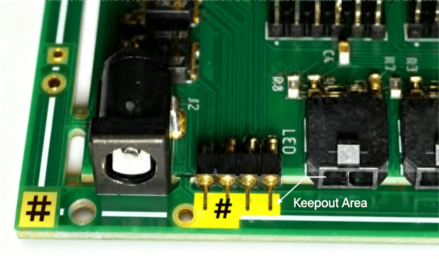
Multilayer PCB
Core Principles, Advantages, Design Basics & HCJMPCBA’s Manufacturing Solutions
Introduction

1. Core Fundamentals of Multilayer PCB
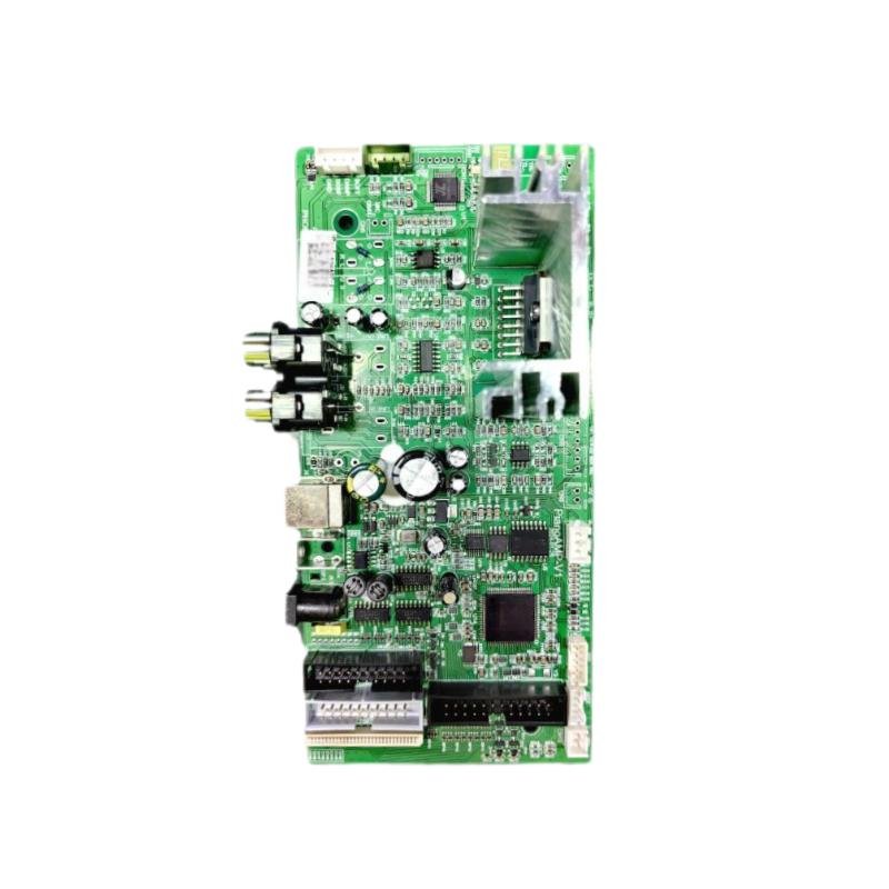
1.1 Key Components of Multilayer PCB
| Component | Description | HCJMPCBA Specification |
|---|---|---|
| Substrate (Core) | Insulating base providing mechanical rigidity. | FR-4 (Tg 140°C/170°C/180°C), halogen-free FR-4, Rogers 4350B |
| Copper Layers | Conductive layers for signals, power, or ground. | 0.5oz–6oz copper weight; 3mil/3mil trace/space |
| Vias | Holes connecting layers (through-hole, blind, buried). | Through-hole (6mil drill), blind/buried (4mil laser drill) |
1.2 Multilayer PCB Manufacturing Workflow
- Inner Layer Patterning: Etch copper on core layers; inspect via AOI (Automated Optical Inspection).
- Layer Stacking: Align inner layers with prepreg and outer copper-clad substrates; use laser alignment (±25μm accuracy).
- Lamination: Press stack at 180–200°C and 250–400 psi to form a monolithic board.
- Drilling: CNC drill through-hole/blind vias; laser drill microvias for high-density designs.
- Plating: Electroplate vias with 20–30μm copper to ensure layer connectivity.
- Outer Layer Processing: Etch outer copper, apply solder mask/silkscreen; test via flying probe/ICT.
2. Advantages & Disadvantages of Multilayer PCB
| Aspect | Advantages | Disadvantages |
|---|---|---|
| Size & Density | 50% smaller footprint vs. single-layer PCBs; supports high-pin-count components (e.g., BGA) | Higher upfront design costs (requires SI/EMC simulation) |
| Electrical Performance | Reduced EMI (60–80% less crosstalk via ground planes); controlled impedance (±5%) | Complex manufacturing (longer lead times: 5–10 days vs. 2–3 days for single-layer) |
| Reliability | Laminated structure resists vibration (MIL-STD-883H compliant); better thermal dissipation | Difficult rework (inner layers inaccessible; errors lead to scrap) |
| Cost Efficiency | Lower total cost of ownership (TCO) in high-volume production (fewer connectors) | Higher material costs (e.g., Rogers is 5–10x more expensive than FR-4) |
HCJMPCBA Mitigation: We offer free DFM (Design for Manufacturability) reviews to reduce rework risks and expedited multilayer pcb manufacturing (3–5 days for 4–6 layer boards) to shorten lead times.

3. Multilayer vs. Single-Layer PCB: Key Advantages
Single-layer PCBs work for basic electronics (e.g., LED lights), but multilayer printed circuit technology outperforms them in complex, high-performance applications. The table below quantifies the differences.
| Performance Metric | Single-Layer PCB | Multilayer PCB (4-Layer, HCJMPCBA) |
|---|---|---|
| Wiring Density | ~10 traces/sq.in | ~50 traces/sq.in |
| EMI Suppression | Poor (-20dB to -30dB crosstalk) | Excellent (-50dB to -60dB crosstalk) |
| Power Distribution | Discrete traces (high voltage drop) | Dedicated power planes (±2% voltage stability) |
| Thermal Management | Hotspots (25–30°C temperature rise) | Copper planes (10–15°C temperature rise) |
| Application Suitability | Basic consumer electronics | Medical devices, 5G, automotive ADAS |
Case Study: A client’s industrial sensor using a single-layer PCB experienced 20% signal loss. HCJMPCBA converted it to a 4-layer multilayer pcb board, cutting signal loss to 3% and reducing size by 40%.
4. 4-Layer, 6-Layer & 8-Layer PCB Design Basics
4.1 4-Layer PCB Design (Most Popular)
| Design Aspect | Details |
|---|---|
| Standard Stackup | Top (Signal) → GND Plane → Power Plane → Bottom (Signal) |
| Key Considerations |
– Assign high-speed signals to top/bottom layers (short paths). – Use internal planes for 3.3V/5V power; avoid splitting ground planes. |
| HCJMPCBA Capabilities |
– Min trace/space: 3mil/3mil – Lead time: 3–5 days – Applications: 5G routers, portable medical monitors |
4.2 6-Layer PCB Design (High-Speed/High-Power)
| Stackup Configuration | Layer 1 | Layer 2 | Layer 3 | Layer 4 | Layer 5 | Layer 6 |
|---|---|---|---|---|---|---|
| Config 1 (Signal-Centric) | Signal | GND Plane | Signal | Signal | Power Plane | Signal |
| Config 2 (Power-Centric) | Signal | GND Plane | Power Plane | Signal | GND Plane | Signal |
| HCJMPCBA Tips | – Use symmetric stackups to prevent warping. – Add thermal vias under MOSFETs (0.3mm drill). – Impedance control: ±5% for PCIe 4.0 | |||||
4.3 8-Layer PCB Design (Ultra-High Performance)
| Design Focus | Recommendations |
|---|---|
| Stackup Optimization | Top (RF Signal) → GND → High-Speed Signal → Power → GND → Low-Speed Signal → Power → Bottom (Control) |
| Manufacturing Needs | – Sequential lamination for inner layer alignment.
|
| HCJMPCBA Expertise | – Supports Rogers 4350B for RF layers.
|
4.4 Design Comparison: 4-Layer vs. 6-Layer vs. 8-Layer
| Feature | 4-Layer PCB | 6-Layer PCB | 8-Layer PCB |
|---|---|---|---|
| Cost (100pcs, 100×100mm) | $1.5–$2.0/unit | $2.5–$3.5/unit | $4.0–$6.0/unit |
| Signal Layers | 2 (top/bottom) | 4 (2 inner + 2 outer) | 6 (4 inner + 2 outer) |
| EMI Performance | Good (-50dB crosstalk) | Very Good (-55dB crosstalk) | Excellent (-60dB crosstalk) |
| Power Domains Supported | 1–2 (3.3V/5V) | 3–4 (1.8V/3.3V/5V/12V) | 5–6 (multiple low-voltage rails) |

5. Applications of Multilayer PCB Across Industries
Multilayer pcbs are ubiquitous in modern electronics, enabling miniaturization and high performance. HCJMPCBA tailors solutions to industry-specific needs.
| Industry | Application Examples | Required Layers | HCJMPCBA Solution Highlights |
|---|---|---|---|
| Consumer Electronics | Smartphones, laptops, smartwatches | 6–12 layers | Microvias (0.1mm) for compact designs; ENIG surface finish |
| Medical Devices | X-ray machines, heart monitors, glucose sensors | 8–16 layers | ISO 13485 compliant; biocompatible solder mask |
| Automotive | ADAS radar, BMS, infotainment systems | 8–12 layers | High-Tg FR-4 (≥180°C); CISPR 25 EMI compliant |
| Telecommunications | 5G base stations, routers, satellite modules | 10–24 layers | Rogers 4350B for RF layers; ±3% impedance control |
| Industrial | PLCs, motor drives, sensor modules | 4–8 layers | Vibration-resistant lamination; 6oz copper for high-current |
Keyword Integration: HCJMPCBA’s pcb manufacturing multilayer services support these applications with custom multi layer circuit boards and rapid prototyping.
6. Why Are Multilayer PCBs Widely Used?
The global multilayer pcb market grows at 15% annually (Prismark 2025) due to irreversible industry trends. Below is why they’ve replaced single-layer PCBs in most advanced electronics.
| Trend | Driver for Multilayer PCB Adoption |
|---|---|
| Device Miniaturization | Consumers demand smaller gadgets (e.g., wearables). Multilayer pcb reduces size by 50% vs. single-layer. |
| High-Speed Signals | 5G (28GHz), DDR5 (4800Mbps) require controlled impedance—only possible with dedicated ground/power planes in multilayer printed circuit boards. |
| Regulatory Compliance | Medical/automotive standards (ISO 13485, ISO 26262) mandate low EMI—achieved via multilayer circuit board shielding. |
| Cost Efficiency (Volume) | In high-volume production (10k+ units), multilayer pcb manufacturing cuts TCO by 25% (fewer connectors, lower failure rates). |
HCJMPCBA Insight: Our clients report 30% faster time-to-market by using multilayer pcbs to avoid redesigns during mass production.

7. Cost Optimization Strategies for Multilayer PCB
While multilayer pcb has higher upfront costs, HCJMPCBA’s strategies reduce total expenses without compromising quality.
| Optimization Area | Actionable Tips | HCJMPCBA Support |
|---|---|---|
| Layer Count | Use 4-layer instead of 6-layer if possible (saves 30% cost). Audit signal needs to avoid over-engineering. | Free stackup analysis to recommend minimal necessary layers. |
| Material Selection | Use FR-4 for non-RF designs; limit Rogers to critical RF layers (reduces material costs by 40%). | Hybrid stackups (FR-4 + Rogers) for cost-performance balance. |
| Panelization | Maximize board count per panel (e.g., 20x 50x50mm boards on 500x500mm panel). | In-house panelization tool to optimize layout. |
| Via Optimization | Use through-hole vias instead of blind/buried (saves 15% manufacturing cost). | DFM review to eliminate redundant vias. |
| Order Consolidation | Combine multiple prototype orders into one (volume discount: 10–20% off). | Custom volume pricing for 100+ unit orders. |
7.1 Cost Comparison: Optimized vs. Non-Optimized
| Scenario | 4-Layer PCB (100pcs, 100x100mm) | 6-Layer PCB (100pcs, 100x100mm) |
|---|---|---|
| Non-Optimized (Blind Vias, Rogers) | $350 | $600 |
| Optimized (Through-Hole, FR-4) | $245 (30% savings) | $420 (30% savings) |
8. Common Design Pitfalls & Solutions
Even experienced engineers face challenges in multilayer pcb design. HCJMPCBA’s DFM reviews catch 90% of issues before production.
| Pitfall | Impact | HCJMPCBA Solution |
|---|---|---|
| Poor Stackup Design | High crosstalk (-30dB); EMI failures | Symmetric stackups (e.g., Signal-GND-Power-Signal for 4-layer); SI simulation. |
| Ignoring Impedance Control | Signal reflection; data errors (e.g., USB 3.0) | Impedance calculator (based on material Dk/copper weight); ±5% tolerance testing. |
| Inadequate Thermal Vias | Component overheating (120°C); premature failure | Thermal via arrays (0.3mm drill, 1mm spacing) under power components; 2oz copper planes. |
| Split Ground Planes | Broken signal return paths; EMI emissions | Continuous ground planes; star grounding for analog/digital separation. |
| Incorrect Via Placement | Parasitic capacitance; signal delay | Vias placed at trace ends (not mid-signal); buried vias for inner-layer connections. |
8.1 Troubleshooting Table for Common Issues
9. HCJMPCBA’s Multilayer PCB Capabilities
| Symptom | Root Cause | Fix |
|---|---|---|
| Signal Reflection | Impedance mismatch (e.g., 45Ω vs. 50Ω) | Adjust trace width (0.2mm for 50Ω on FR-4); add termination resistors. |
| Board Warping | Asymmetric stackup (e.g., 2oz vs. 1oz copper) | Symmetric copper weight; balanced layer count (even layers). |
| Via Open Circuits | Insufficient plating (≤15μm) | 20–30μm copper plating; X-ray inspection for via connectivity. |
As a full-service multilayer pcb supplier, HCJMPCBA combines technical expertise with customer-centric support to deliver reliable solutions.
| Capability | Specification |
|---|---|
| Layer Count | 2–32 layers (supports 40-layer custom projects) |
| Material Options | FR-4 (Tg 140–180°C), halogen-free FR-4, Rogers 4350B/4003C, polyimide (flex) |
| Manufacturing Tolerances | Trace/space: ±0.05mm; board thickness: ±10%; impedance: ±5% |
| Surface Finish | HASL (lead-free), ENIG, immersion silver/tin, OSP |
| Quality Standards | IPC-A-600 Class 2/3, ISO 9001, ISO 13485 (medical), RoHS |
| Lead Time | 3–5 days (4-layer); 5–7 days (6-layer); 7–10 days (8-layer); expedited 1–2 days |
| Testing | AOI, X-ray, flying probe, ICT, functional testing, thermal cycling (-40°C to +125°C) |
Conclusion
Multilayer pcb technology is the backbone of modern electronics—enabling miniaturization, high-speed performance, and regulatory compliance. As a leading multilayer pcb manufacturer, HCJMPCBA’s expertise in multilayer pcb design and cost optimization ensures your project meets performance goals while staying on budget. Whether you need a 4-layer consumer PCB or a 32-layer aerospace board, we deliver solutions tailored to your industry’s unique needs.

