
What Is Medical PCB Assembly—and How to Navigate the Medical PCB Supply Chain?
Medical PCB assembly is essential for creating reliable, high-precision electronic medical component
Medical PCB assembly is essential for creating reliable, high-precision electronic medical component
Guangzhou Huachuang Precision Technology ensures high PCBA reliability through advanced SMT and BGA
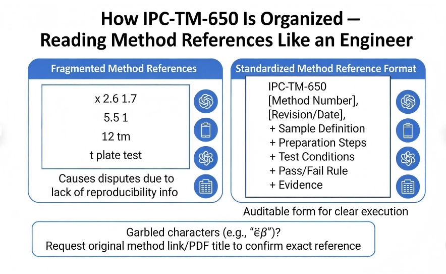
What is ipc-tm-650 and how does it help PCB and PCBA teams control quality with consistent, comparab


