In the high‑stakes world of medical electronics, every trace, every component, and every solder joint can mean the difference between life and failure. HCJMPCBA has honed a medical PCB assembly process that transcends conventional manufacturing. Backed by ISO 13485 certification and IPC Class 3 compliance, our end‑to‑end approach delivers reliability that critical medical devices demand.
Medical‑Grade Quality Assurance for PCB Assembly Medical Device
1.1 Understanding the Stakes of Medical PCB Assembly
Unlike consumer electronics, medical pcb assembly must guarantee absolute traceability, stringent risk management, and zero‑defect output. Regulatory bodies such as the FDA and EU MDR compel manufacturers to document every material source, in‑process inspection, and final functional test. At HCJMPCBA, we embed these requirements into our DNA:
-
Material Qualification
-
Biocompatibility (USP Class VI): All substrates and encapsulants undergo cytotoxicity, sensitization, and irritation testing.
-
RoHS & REACH Compliance: Verifiable certificates for heavy metal limits and restricted substances to avoid patient harm.
-
Process Validation
-
Controlled Environment: Class 7 cleanrooms with temperature and humidity governance ensure no particulate contamination.
-
Equipment Calibration: Our Panasonic NPM‑W2 pick‑and‑place and DEK Horizon 03iX screen printers are recalibrated monthly, maintaining ±25 µm placement accuracy.
-
Inspection & Traceability
-
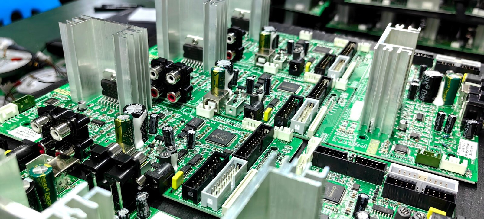
3D AOI captures solder joint volume and fillet shape on implantable device PCBs, alerting operators to voids or bridging before reflow.
-
X‑Ray Analysis post‑reflow for BGA and micro‑BGA packages, guaranteeing hidden interconnect integrity.
-
Barcode‑Driven Tracking: Each panel carries a unique serial, logged in our MES—every step from stencil print to final test is time‑stamped and archived.
1.2 Final Validation: Functional Testing Beyond the Surface
Final inspection is not perfunctory—it’s exhaustive:
-
Electrical Testing: ICT verifies net connectivity; FCT simulates real device loads.
-
Environmental Stress Screening: Thermal cycling (–40 °C to +125 °C) and 85 % RH soak for 500 hours expose latent defects.
-
Mechanical Integrity: Vibration and shock tests replicate transport and in‑body conditions for wearables.
This triple‑layer validation ensures our pcb assembly medical device boards perform faultlessly in their intended clinical settings.
2: Certified Expertise Across Medical, AI & Industrial PCB Domains
HCJMPCBA’s competence is not confined to medical electronics. Cross‑industry experience reinforces our custom pcb design for medical devices:
2.1 Medical Focus: Tailored Design for Patient Safety
-
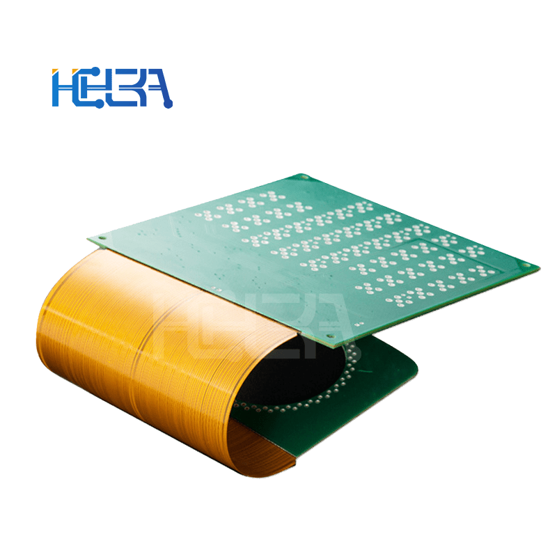
Wearable Devices: Low‑profile flex PCBs with polyimide substrates withstand body flex and moisture ingress.
-
Diagnostic Equipment: Multilayer rigid boards incorporate dedicated ground planes and isolation barriers to meet IEC 60601‑1 safety requirements.
-
Implantable Controllers: Ultra‑miniature substrates with gold‑plated vias ensure corrosion resistance within physiological environments.
2.2 AI Hardware: HDI PCB Assembly for High‑Performance Computing
-
20‑Layer HDI Stacks: Controlled impedance routing and blind/buried vias support GHz‑class signaling on GPU and CPU boards.
-
Liquid‑Cooling Interfaces: Conformal copper pours and thermal vias integrate with liquid heat sinks to manage 400+ W power densities.
2.3 Industrial Automation: Ruggedized Reliability
-
IPC Class 3 PCBA: Highest workmanship class suited for mission‑critical machinery, with reinforced through‑hole solder joints and conformal coatings.
-
IP67 Modules: Sealed assemblies resistant to dust, moisture, and chemical spray for factory‑floor deployments.
By carrying lessons across sectors, our medical pcb production benefits from AI and industrial innovations—yielding boards that are not only safe, but also cutting‑edge.
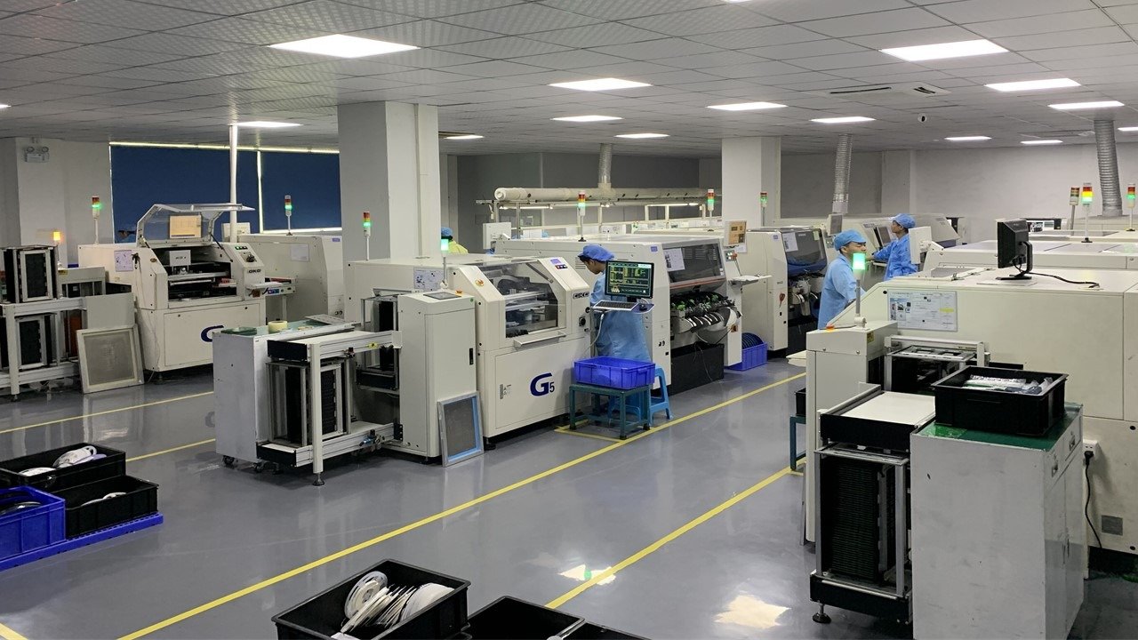
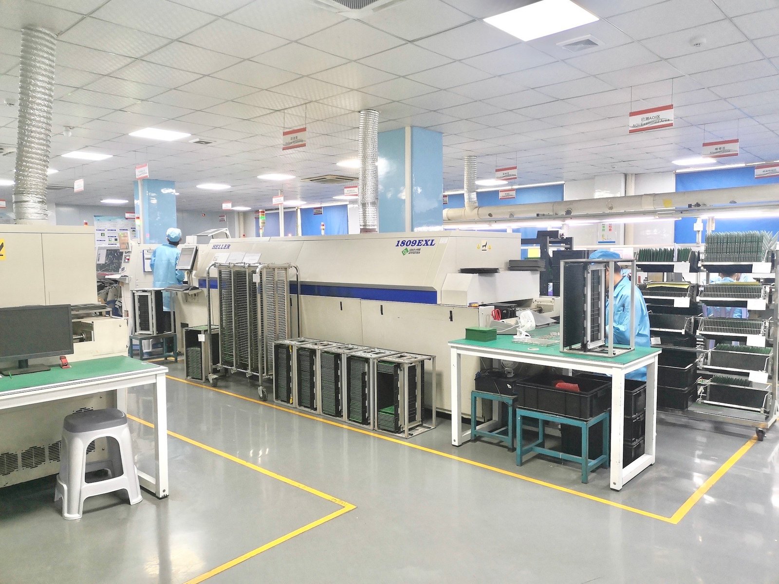
3: Advanced Facilities & Precision Equipment for Medical PCB
Precision at scale demands best-in-class machinery and controls:
-
Panasonic NPM‑W2: 50,000 CPH for consistent placement of 0201–0402 components used in compact medical sensors.
-
DEK Horizon 03iX: ±25 µm stencil printing precision, critical for micro‑BGA pad definition.
-
Yamaha YSi: Intelligent vision correction achieves sub‑30 µm alignment on flex PCBs destined for catheters and wearables.
Environmental and static controls:
-
Cleanroom Class 7: Limits airborne particles to <352,000 particles/m³ at 0.5 µm.
-
ANSI/ESD S20.20 Compliance: Ionization and grounding systems protect sensitive ICs from electrostatic discharge.
Testing apparatus:
Together, these assets ensure every medical pcb assembly meets rigorous quality thresholds before leaving the factory.
4: Customized Solutions & Efficient Supply Chain
Selecting a PCB partner goes beyond process mastery—it’s about adaptability and speed:
-
Rapid Prototyping & DFM
-
3–5 Day Turnaround on low‑volume prototypes for preclinical trials.
-
DFM Workshops: Collaborative sessions to refine pad geometry, trace widths, and layer stack‑ups—reducing expensive redesign loops by 25 %.
-
Component Authentification & Sourcing
-
Global Logistics & Compliance
-
DHL Express and FedEx Priority options for USA/Europe shipments, meeting 7–14 day lead times.
-
Regulatory Documentation Packs: Include full traceability, material certifications, and test records to streamline audits and device submissions.
This efficient supply chain underpins consistent delivery of compliant medical pcb assemblies.
5: Why Partner with HCJMPCBA for Medical PCB Assembly?
Choosing a medical PCB supplier is choosing a collaborator in patient safety:
-
Proven Track Record
-
100+ FDA‑approved device integrations, from glucose monitors to implantable neurostimulators.
-
99.99 % first‑pass yield under ISO 13485 controls.
-
Cross‑Industry Synergy
-
Continuous Innovation
Our commitment to excellence makes HCJMPCBA more than a contract manufacturer—we’re your strategic partner in life‑critical electronics.
Conclusion
Medical PCB assembly is an intricate tapestry of regulatory vigilance, meticulous process control, and advanced engineering. HCJMPCBA’s ISO 13485‑certified framework fuses biocompatible materials, precision equipment, and cross‑sector expertise to deliver boards that power life‑saving devices with unfailing reliability.
Call to Action
Ready to elevate your next medical device? Request a quote or schedule a facility tour with HCJMPCBA today. Let’s collaborate on custom PCB design, turnkey SMT processing, or rapid‑turn prototyping—and ensure your products meet the highest standards of safety and performance.
To learn more about PCBA services, please contact Guangzhou Huachuang Precision Technology.