Small Water Pumps: 12 Expert Steps to Make a Reliable Mini Water Pump (2025 Updated Guide)
Discover what small water pumps are, its core types (submersible, solar, electric), and key applicat
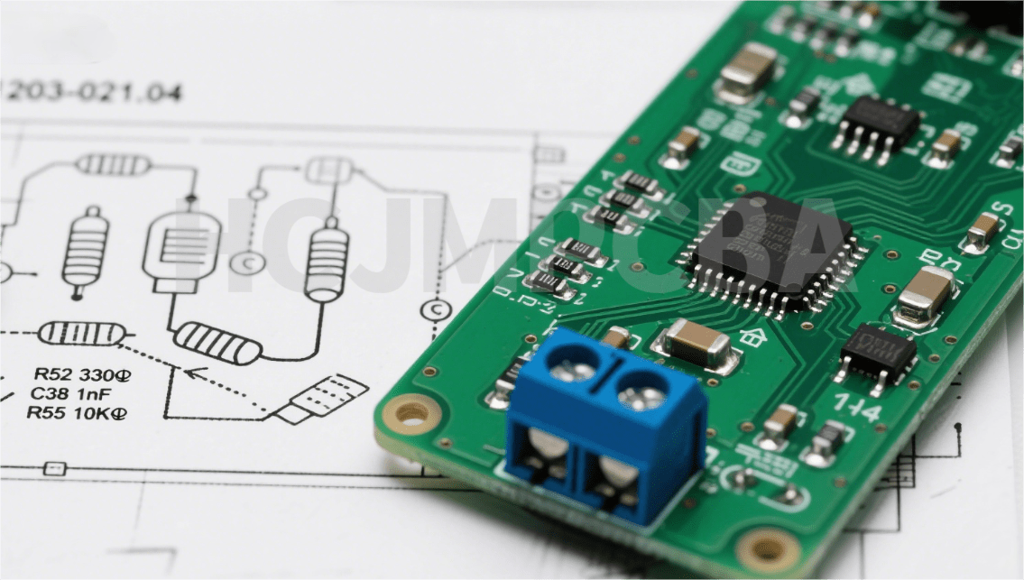
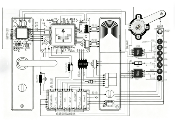
Schematic Drawing Design Of Electronic Circuit Board | HCJMPCBA
Schematics (also known as schematic diagrams, electrical schematics, or circuit schematics) are the universal language of electronics. Understanding what schematics are and how to read schematic diagrams is foundational for OEM engineers, purchasers, and anyone working in PCBA or electronic manufacturing services. Whether you want to know how to read wiring schematics, schematic circuit diagram, or printed circuit board schematics, this guide walks you through symbols, diagrams, and techniques to interpret and apply schematics with clarity.
A schematic, or schematic diagram, is a structured representation of a system using abstract graphic symbols rather than realistic images. Its purpose is to emphasize functionality and relationships—much like a subway map that uses simple symbols to convey routes rather than realistic geography. In electronics, schematics abstract components (resistors, capacitors, ICs, etc.) into symbols to convey circuit intentions clearly.
In electronics design, especially for PCB or PCBA projects, schematics serve two primary purposes:
Communicating design intent—showing how the circuit should function.
Providing a blueprint for PCB layout and manufacturing by translating schematic capture into a netlist used by design tools.
Although often treated interchangeably, a schematic diagram focuses on connectivity using standardized symbols, while a circuit diagram may attempt to represent wiring layout. The PCB layout, in contrast, shows the actual physical placement of components and traces. Schematics are conceptual, while layouts are physical; both are essential in PCB/PCBA workflows.
Schematics rely on standardized electronic symbols—such as resistor zigzags, capacitor lines, and transistor shapes—to keep diagrams universally interpretable. These symbols follow international standards like IEC 60617 and ANSI/Y32.2.
Each component is labeled with a unique reference designator (e.g., R1, C3, U5), which identifies its type and links to the Bill of Materials (BOM). REFDES makes BOM tracking and component identification much easier.
Lines (nets) connect component pins, representing signal or power paths. Common conventions: signal flow left-to-right, power rails at top, ground at bottom. Many schematics use annotations, net labels, and grid alignment for readability.
1.Identify Functional Blocks – Break the schematic into logical modules like power, amplifier, connector.
2.Recognize Symbols & Follow Net Labels – Understand each icon and trace labels to follow signal paths.
3.Trace Signal Flow – Read from input to output: left to right, top to bottom.
4.Cross-Reference REFDES with BOM – Match symbols to components in the BOM to ensure correct parts.
5.Review Annotations, Title Block, Revision History – Look for notes that impact function or changes over time.
Single-Line Diagrams (especially in power systems) simplify multi-phase circuits into one representative line.
Multi-Line Diagrams show each conductor separately.
Block / Interconnect Diagrams help visualize modular system layouts at a high level.
Use grid alignment, clear label conventions, and page titles/headers including revision data.
Employ schematic capture tools (e.g., in EDA software like KiCad, Altium) to generate clean, standardized diagrams and netlists.
Organize schematic pages logically and break complex designs into separate sheets labeled alphabetically.
Q: What to check when reviewing a schematic?
F: Verify symbols, REFDES, correct nets/power, annotations, BOM alignment.
A: Apply reading steps, compare with BOM, ensure clarity and revisions are noted.
What are schematics used for?
To communicate circuit design, guide PCB layout, and facilitate maintenance.
How does a schematic differ from a circuit diagram?
Schematics abstract functionality; circuit diagrams may show layout or physical wiring.
What key symbols should I know?
Resistors (zigzag or rectangle), capacitors (parallel lines), diodes, transistors, connectors.
How do I transition from schematic to manufacturing?
Use schematic capture to generate netlists and Gerber files for production.
Any advice on reading complex schematics?
Break into blocks and trace signal flows one section at a time.
To learn more about PCBA services, please contact Guangzhou Huachuang Precision Technology.
Discover what small water pumps are, its core types (submersible, solar, electric), and key applicat
Discover what a circuit diagram is and how to read or design a clear pcb schematic step-by-step. Und
This guide explains how to import component in altium in a production-ready way—so imported parts