PCB Prototyping Process | HCJMPCBA
Introduction
PCB prototyping acts as the vital nexus between electronic design conceptualization and mass production scalability—a stage essential for validating circuit functionality, performance, and manufacturability before full-scale manufacturing begins. At HCJMPCBA, our engineered prototyping workflow balances agile turnaround, precision engineering, and cost-optimization, serving demanding sectors like medical device development, industrial automation control systems, AI hardware innovation, and aerospace electronics.

Step 1: Comprehensive Design Review & DFM Analysis
Before production starts, our cross-functional engineering team conducts a rigorous Design for Manufacturability (DFM) assessment:
- Scrutinize Gerber files, Bill of Materials (BOM), and design schematics for dimensional accuracy, layer alignment, and compliance with IPC-2221/2222 standards.
- Proactively spot potential issues (e.g., insufficient trace spacing for high-speed signals, component footprint mismatches, solder mask clearance violations) to eliminate rework cycles.
- Deliver customized recommendations to optimize the design for prototyping throughput (e.g., panelization strategies) and volume production yield (e.g., test point placement for ICT).
Why it matters: Fixing design flaws at this early stage cuts revision cycles by up to 70%, reducing both time-to-market and non-recurring engineering (NRE) costs.
Step 2: Strategic Material & Component Sourcing
We select materials and components to meet your project’s technical and regulatory needs:
- Material Selection: Use FR-4 (standard/halogen-free), high-Tg FR-4 (for thermal endurance), Rogers laminates (for RF/high-frequency applications), or aluminum-backed PCBs (for thermal management) based on thermal, mechanical, and electrical performance criteria.
- Component Procurement: Secure 100% authentic active/passive components via authorized distributors (Mouser, DigiKey, Avnet) with anti-counterfeit verification; offer BOM kitting for turnkey prototyping to simplify assembly.
- Regulatory Compliance: Ensure materials meet RoHS, REACH, and industry-specific standards (e.g., ISO 13485 for medical devices, AS9100 for aerospace) to enable smooth scale-up.
Why it matters: High-quality material and component sourcing ensures prototypes accurately replicate the form, fit, and function of mass-produced units—critical for reliable validation testing.
Step 3: Precision-Driven PCB Fabrication
Our fabrication process combines advanced machinery with Statistical Process Control (SPC) to ensure structural integrity:
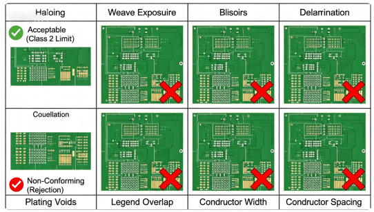
- Core Processes: Layer lamination (up to 8 layers), CNC drilling (tolerances ±0.05mm), chemical copper etching (etch factor <1.2 for fine features), and solder mask application (coverage uniformity ±5µm) follow IPC-A-600 Class 2/3 standards.
- Advanced Capabilities: Support fine-line geometries (down to 3mil trace/space), microvias (0.1mm diameter), and hybrid constructions (rigid-flex, metal-core PCBs) for complex designs.
- In-Line Inspection: Use Automated Optical Inspection (AOI) for surface defects, X-ray inspection for BGA/QFN solder joint integrity, and impedance testing (±5% tolerance) for high-speed signal integrity.
Why it matters: Precision fabrication ensures the prototype’s electrical characteristics (e.g., impedance, crosstalk) and mechanical durability match design simulations—enabling trustworthy performance validation.

Step 4: Flexible Assembly (SMT/DIP/Hybrid)
For prototypes needing component integration, we offer versatile assembly solutions:
- Surface Mount Technology (SMT): High-speed pick-and-place systems (±25µm placement accuracy) handle ultra-fine pitches (01005, 0.3mm BGA) and advanced packages (QFN, LGA).
- Through-Hole (DIP) Assembly: Manual/automated insertion for connectors, power modules, and legacy components; wave soldering for high-throughput through-hole processing.
- First Article Inspection (FAI): Verify assembly accuracy against IPC-A-610 Class 2/3 acceptability criteria before full-batch processing to reduce defect spread.
Why it matters: Professional assembly turns bare PCBs into functionally testable units, speeding up the transition from design to real-world validation.
Step 5: Rigorous Testing & Validation
Prototypes go through multi-level testing to ensure reliability and compliance:
- Electrical Verification: In-Circuit Testing (ICT) for net connectivity/shorts, flying probe testing for high-density boards, and boundary scan testing for JTAG-compliant devices.
- Functional Validation: Custom test fixtures and software simulate end-use scenarios (e.g., power cycling, signal transmission at rated frequencies) to confirm operational conformance.
- Environmental Screening (Optional): Temperature cycling (-40°C to +125°C), vibration testing (per MIL-STD-202), and humidity testing (85% RH/85°C) to assess ruggedness for industrial/aerospace applications.
Why it matters: Thorough testing reduces mass production risks by identifying design flaws (e.g., thermal hotspots, signal integrity issues) that only appear under real-world stress.

Step 6: Streamlined Delivery & Iteration Enablement
- Accelerated Turnaround: Standard prototypes ship in 3–5 business days; expedited services (1–2 days) are available for time-critical projects.
- Documentation & Insights: Provide test reports (ICT results, X-ray images), inspection logs, and DFM feedback to guide iterative design improvements.
- Engineering Collaboration: Our team works with you to analyze prototype performance data and refine designs for manufacturability, cost, or performance gains.
Why it matters: Efficient delivery and post-prototype support keep your product development cycle agile, minimizing delays between iterations.
Making the Optimal Choice: Decision-Making Framework for PCB Prototyping
Project Needs Evaluation
Timeline Prioritization
- How urgent is the prototype delivery (e.g., 48-hour rush, 5-day standard, or flexible timeline)?
- What business impacts stem from delayed delivery (e.g., market launch setback, R&D cycle extension)?
- Is there flexibility to adjust the schedule if trade-offs (cost, quality) become necessary?
Quality Expectations
- What is the prototype’s intended use (e.g., lab validation, field demo, pre-production pilot)?
- Must it meet specific industry standards (e.g., IPC-A-600 Class 3, ISO 13485 for medical, MIL-STD for aerospace)?
- How critical is “first-pass success” to avoid costly redesign cycles?
Budget Allocation
- What is the total budget allocated for prototyping (including contingency funds)?
- How does prototyping cost influence the overall project’s financial viability?
- Are there opportunities to optimize costs (e.g., simplifying non-critical features for prototyping)?
Technical Complexity
- How intricate is the PCB design (layer count, trace density, high-speed signal requirements)?
- Are specialized materials needed (e.g., Rogers laminates for RF, flexible substrates, metal-core PCBs)?
- What performance parameters are non-negotiable (e.g., impedance control, thermal management)?
Manufacturer Evaluation Criteria
Reliability & Industry Expertise
- Historical on-time delivery rate for projects with similar complexity?
- Client testimonials and case studies (especially in your target industry)?
- Years of experience navigating technical challenges in PCB prototyping?
Technical Competence
- Compatibility with your design rules (e.g., minimum trace/space, via dimensions)?
- Range of material options and ability to support quick-turn requests?
- Rigor of quality control processes (e.g., AOI, X-ray inspection, electrical testing)?
Collaboration & Support
- Responsiveness to inquiries (e.g., RFQ turnaround, technical question resolution)?
- Availability of engineering support (e.g., DFM feedback, design optimization guidance)?
- Transparency in project status updates (e.g., milestone tracking, delivery estimates)?
Cost Transparency
- Clarity in pricing breakdown (fabrication, assembly, testing costs)?
- Risk of hidden fees (e.g., setup charges, revision penalties)?
- Predictability of shipping, duty, and import costs (for international projects)?
Risk Management Approaches
Contingency Planning
- Identify secondary manufacturers with matching technical capabilities?
- Build buffer time into project timelines to account for unforeseen delays?
- Explore parallel workflows (e.g., material sourcing while design is finalized)?
Quality Safeguards
- Verify manufacturer certifications (e.g., ISO 9001, UL) before engagement?
- Implement incoming inspection protocols for received prototypes?
- Allocate time for in-house validation testing after prototype delivery?
Communication Framework
- Define primary and backup contact points for both teams?
- Agree on update frequency (e.g., daily/weekly) and format (e.g., email, project portal)?
- Establish a clear escalation path for issues (e.g., engineer → account manager → leadership)?
Why Choose HCJMPCBA’s Prototyping Process?
- Precision-at-Speed: Achieve IPC Class 3-quality prototypes with turnaround times 30% faster than industry averages.
- Vertical Integration: In-house capabilities (design review → fabrication → assembly → testing) eliminate dependence on third-party vendors, ensuring quality control and timeline predictability.
- Industry-Centric Expertise: Deep domain knowledge in medical (ISO 13485-certified), industrial (UL 60950 compliance), and high-tech sectors to address niche technical needs.
- Cost Optimization: Low minimum order quantities (MOQs start at 5 pieces) and early defect detection reduce the total cost of ownership (TCO) for prototyping campaigns.
| Features | Capability |
|---|---|
| Guangzhou-Based Precision | Locally rooted in Guangzhou’s tech hub, our manufacturing facility ensures strict process control and proximity to supply chains for enhanced prototype accuracy. |
| Expedited Prototyping | Optimized workflows enable quick turnaround times, with options for 24-72 hour rush services to accelerate your product development cycle. |
| Advanced Testing Protocols | In-house testing labs with cutting-edge equipment verify functionality, ensuring each prototype meets IPC and industry-specific standards. |
| Flexible Customization | Supports a wide range of materials (FR-4, Rogers, etc.), layer counts (2-32 layers), and finishes, tailored to your unique design specifications. |
| Online Order Transparency | User-friendly online platform allows instant quoting, order tracking, and direct communication with engineers for seamless project management. |
| Cost-Optimized Solutions | Competitive pricing structure with transparent costs, ideal for startups and enterprises alike, without compromising on precision or reliability. |