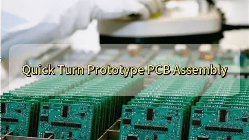
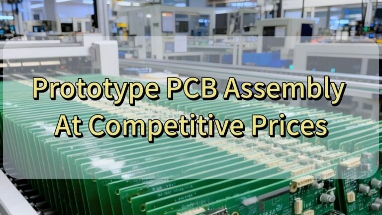
Prototype PCB Assembly
Accelerate Your Product Development with HCJMPCBA’s Expert Solutions
Introduction: The Critical Role of Prototype PCB Assembly
Understanding Quick Turn Prototype PCB Assembly
- Validate design concepts swiftly
- Identify and resolve design flaws early
- Accelerate the iteration cycle
- Gain a competitive edge by launching products faster
Our Prototype PCB Assembly Services
1. Surface Mount Technology (SMT) Assembly
- Placement of components as small as 01005 (for advanced prototypes)
- Precision soldering using reflow and wave processes
- Support for fine-pitch components (down to 0.3mm pitch)
- Compatibility with leaded and lead-free solder materials
2. Through-Hole (DIP) Assembly
- Manual and automated insertion of through-hole components
- Wave soldering for consistent, high-quality joints
- Support for odd-form and custom components
3. Mixed Technology Assembly
- Precise alignment and soldering of mixed-component layouts
- Validation of interconnections between SMT and through-hole sections
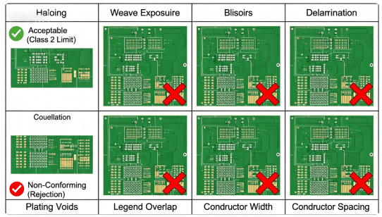
- Compliance with IPC-A-610 Class 2/3 standards
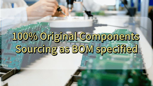
4. Component Sourcing and Procurement
- Procurement of active and passive components from authorized distributors
- Management of bill-of-materials (BOM) for accuracy and cost-efficiency
- Provision of alternative components (with client approval) to avoid delays
- Management of component lifecycle and obsolescence risks
5. Testing and Inspection
- Automated Optical Inspection (AOI) for solder joint and component verification
- X-ray Inspection for hidden via and BGA connectivity checks
- Functional Testing (FT) to validate circuit performance
- In-Circuit Testing (ICT) for comprehensive electrical verification
| Service Type | Key Capabilities | Ideal For | Typical Lead Time |
|---|---|---|---|
| SMT Assembly | 01005 component placement, fine-pitch soldering | High-density, compact prototypes | 24–72 Hours |
| Through-Hole (DIP) Assembly | Wave soldering, odd-form component support | Power electronics, mechanical fixtures | 48–96 Hours |
| Mixed Technology Assembly | Combined SMT/DIP, IPC-A-610 compliance | Mixed-component prototypes (e.g., IoT devices) | 72–120 Hours |
| Functional Testing | AOI, X-ray, ICT, FT | All prototypes requiring performance validation | 24–48 Hours (after assembly) |
PCB Prototype Lead Time, Quotation and Production Process
PCB Prototype Lead Time
| Prototype Complexity | Standard Lead Time | Expedited Lead Time |
|---|---|---|
| Single-Layer PCB Assembly | 24-48 Hours | 12-24 Hours |
| Double-Layer PCB Assembly | 48-72 Hours | 24-48 Hours |
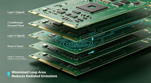
| Multi-Layer (4-8 Layers) | 72-120 Hours | 48-72 Hours |
| HDI/High-Speed PCB | 96-168 Hours | 72-96 Hours |
Note: Lead times depend on component availability, design complexity, and testing requirements. We provide detailed timelines after reviewing your Gerber files and BOM.
Quotation Process
- Submit Your Files: Upload your Gerber files, BOM, and any special requirements (e.g., material preferences, testing needs) via our online portal or email (sales@hcjmpcba.com).
- DFM Review: Our engineers perform a free Design for Manufacturability (DFM) analysis to identify potential issues and optimize for cost and yield.
- Quote Delivery: You’ll receive a detailed quote within 24 hours, including costs for PCB fabrication, component sourcing, assembly, and testing.
- Order Confirmation: Once you approve the quote, we proceed with production.
Production Process
- PCB Fabrication: We manufacture the bare PCB using your Gerber files, adhering to IPC standards.
- Component Sourcing: We procure or verify components based on your BOM.
- Assembly Preparation: Stencils are created, and the assembly line is set up.
- SMT/DIP Assembly: Components are placed and soldered using our advanced equipment.
- Inspection & Testing: The assembled PCB undergoes AOI, X-ray, and functional testing.
- Packaging & Shipping: The finished prototype is packaged and shipped to your location.
Our Technical Capabilities and Why Choose HCJMPCBA as Your Preferred Partner?
Our Technical Capabilities
Advanced Assembly Equipment:
- High-speed SMT pick-and-place machines (capable of 50,000+ components per hour)
- Nitrogen reflow ovens for lead-free and leaded soldering
- Automated optical inspection (AOI) systems for precision verification
- X-ray inspection machines for BGA and hidden via analysis
Material Expertise:
- FR4, Aluminum, Ceramic, and Flexible substrates
- High-Tg (170°C+) and halogen-free materials
- Rogers and other specialty materials for RF and high-speed applications
Quality Standards:
- ISO 9001:2015, ISO 13485, and IATF 16949 certified
- Compliance with IPC-A-610 Class 2/3 for assembly quality
- RoHS and REACH compliant manufacturing
Why Choose HCJMPCBA as Your Preferred Partner?
- Unmatched Speed & Reliability: Our quick turn pcb assembly services deliver prototypes in days, not weeks, without compromising quality. We’ve invested in automated processes to ensure consistency and on-time delivery.
- End-to-End Solutions: From PCB fabrication to pcba assembly, testing, and even box-build, we offer a true one-stop solution. This eliminates the need to coordinate with multiple vendors, saving you time and reducing risks.
- Customization & Flexibility: We understand that every prototype is unique. Our team works closely with you to accommodate custom requirements, whether it’s a specific material, component, or testing protocol.
- Cost-Effective Prototyping: By optimizing panelization, component sourcing, and assembly processes, we offer competitive pricing for prototype pcb assembly without sacrificing quality. Volume discounts are available for repeat projects.
- Industry-Specific Expertise: Our experience spans automotive, medical, industrial, and consumer electronics. We know the regulatory and technical nuances of each industry, ensuring your prototype meets all necessary standards.
- Global Reach & Support: With clients in 50+ countries and a dedicated team for pcb suppliers usa and international markets, we provide localized support and logistics solutions.
Proto PCB Assembly Cost and FAQs
Proto PCB Assembly Cost
- PCB Layers & Complexity: More layers and complex designs (e.g., HDI, blind vias) increase costs.
- Component Type & Quantity: SMD components, fine-pitch parts, and high-value ICs impact pricing.
- Assembly Technology: SMT, through-hole, or mixed technology.
- Testing Requirements: AOI, X-ray, functional testing, etc.
- Volume: Even for prototypes, small batch sizes (1–100 units) can offer cost advantages over single-piece production.
Frequently Asked Questions (FAQs)
We have no strict MOQ—we can assemble a single prototype or small batches (1–100 units) based on your needs.
While we specialize in assembly, we offer DFM reviews and can recommend design improvements. For full PCB design, we can connect you with our partner design firms.
Yes, our component sourcing team has access to global distributors and can locate obsolete parts or suggest suitable alternatives.
We accept Gerber files (RS-274X), BOM in Excel/CSV format, and pick-and-place files (if available).
We follow strict quality control processes, including AOI, X-ray inspection, and functional testing. Our certifications (ISO 9001, etc.) and compliance with IPC standards further guarantee quality.
We offer a 30-day warranty against manufacturing defects. If an issue arises due to our assembly process, we’ll repair or replace the prototype at no cost.