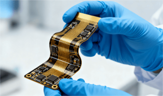
Flexible PCB Manufacturing
HCJMPCBA’s Expert Solutions for Advanced Flexible Circuitry
Introduction: Flexible PCB Manufacturing Services by HCJMPCBA
Our Flexible PCB Manufacturing Capabilities
Flexible PCB Types & Specifications
| Flexible PCB Type | Layers | Material Used | Typical Thickness | Applications | Key Advantages |
|---|---|---|---|---|---|
| Single-Sided Flex PCB | 1 | Polyimide (Kapton), PET | 0.1–0.2mm | Consumer electronics (remote controls, calculators), simple sensors | Low cost, easy fabrication, space-efficient |
| Double-Sided Flex PCB | 2 | Polyimide, with plated-through holes (PTH) | 0.2–0.4mm | Automotive dashboards, medical devices (ECGs), industrial controls | Higher component density, bidirectional wiring, robust connections |
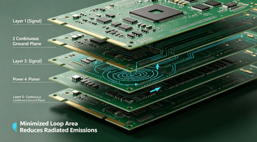
| Multilayer Flex PCB | 3–12 | Polyimide, with buried/blind vias | 0.4–1.0mm | Aerospace equipment, high-end medical devices, AI robotics | Extreme component density, EMI shielding, complex functionality |
| Rigid-Flex PCB | 2–20 (hybrid of rigid and flex layers) | Polyimide + FR4 (rigid sections) | Varies by design | Wearable devices (smartwatches), military gear, automotive infotainment | Combines flexibility and structural stability, reduces assembly steps |
| HDI Flex PCB | 2–8 | Thin polyimide, microvias | 0.3–0.8mm | 5G smartphones, IoT modules, high-frequency RF devices | Ultra-fine pitch routing, miniaturized form factors, high-speed signal integrity |
Advanced Manufacturing Equipment & Processes
- Laser Direct Imaging (LDI): For ultra-fine line widths (down to 25μm) and accurate via placement.
- Automated Optical Inspection (AOI): For real-time quality control during etching and soldering.
- High-Speed Pick-and-Place Machines: For flex pcb assembly of SMT components with 01005 packaging.
- X-Ray Inspection: For verifying hidden vias and BGA solder joints in multilayer flex designs.
Advantages of Flexible PCB: Why Choose Flex Circuits?
Flexible printed circuit boards offer a multitude of benefits that make them indispensable in modern electronics. Here’s a breakdown of their key advantages:
| Advantage | Description | Impact on Product Design |
|---|---|---|
| Space Efficiency | Flex PCBs can bend, twist, and fold, allowing design in tight or irregular spaces. | Enables thinner, more compact devices (e.g., foldable phones, wearable health trackers). |
| Weight Reduction | Lighter than rigid PCBs (no FR4 substrate) and eliminate wiring harnesses. | Critical for aerospace, drones, and portable medical devices where weight is a constraint. |
| Enhanced Reliability | Fewer interconnects reduce failure points; polyimide resists vibration and thermal stress. | Ideal for automotive (engine sensors) and industrial (heavy machinery) applications. |
| Design Flexibility | Supports 3D shaping and custom form factors. | Enables innovative designs like curved automotive dashboards or contoured medical implants. |
| Cost Savings | Reduce assembly steps, wiring, and connector costs; scalable for high-volume production. | Lowers total cost of ownership for consumer electronics and mass-produced industrial gear. |
Common Features of Flexible PCBs (Single, Double, Multilayer)
Despite their structural differences, single-sided, double-sided, and multilayer flexible printed circuit boards share core characteristics that define their performance:
| Feature | Details |
|---|---|
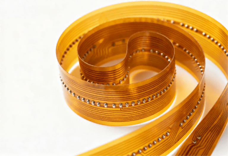
| Base Material | Polyimide (Kapton) is standard for its thermal stability (-269°C to +400°C) and mechanical strength. PET is used for low-cost, less demanding applications. |
| Copper Thickness | Ranges from 0.5oz (17.5μm) to 3oz (105μm), with 1oz (35μm) being the most common for balance of conductivity and flexibility. |
| Surface Finish | Common options: – Immersion Gold (for high reliability, wire bonding) – OSP (for cost-effective, short-term storage) – Immersion Tin (for solderability in high-volume assembly) |
| Cover Layer | Protective polyimide film (adhesive or adhesive-free) that insulates copper traces and provides mechanical protection. Thickness: 12.5–75μm. |
| Bending Radius | Dependent on copper thickness and number of layers. As a rule: – Single-sided: ≥5x board thickness – Multilayer: ≥20x board thickness (Exceeding this can cause copper cracking.) |
| Environmental Resistance | Polyimide-based flex PCBs resist moisture, chemicals, and UV radiation. Custom coatings (e.g., conformal coating) can enhance protection for harsh environments. |
1. Design & Engineering
- DFM Analysis: Our team reviews your Gerber files to optimize for flexible PCB design rules (e.g., minimum trace width, bend radius, via placement).
- Material Selection: We recommend the best substrate (polyimide, PET, etc.) and copper thickness based on your application’s thermal, mechanical, and electrical requirements.
2. Preproduction & Tooling
- Phototool Creation: High-precision phototools are made for each layer of the flex PCB.
- Material Cutting: Large sheets of polyimide and copper are cut to size for your project.
3. Imaging & Etching
- Dry Film Lamination: A photosensitive film is applied to the copper layer.
- Exposure & Development: The design is transferred to the film via UV exposure, then unexposed areas are washed away.
- Etching: Unprotected copper is removed via chemical etching, leaving behind the desired circuit traces.
4. Layer Stacking & Lamination (for Multilayer/Flex-Rigid)
- Alignment & Bonding: Layers are aligned, and adhesive (or adhesive-free bonding) is used to stack them.
- Curing: The stack is cured under heat and pressure to form a single rigid-flex structure.
5. Drilling & Plating (for Double-Sided/Multilayer)
- Via Drilling: Microvias are drilled to connect layers.
- Plating: Vias are metallized to create electrical connections between layers.
6. Cover Layer Application
- Lamination: A protective polyimide cover layer is applied to insulate traces and provide mechanical strength.
- Solder Mask Application: For areas requiring solder resist (optional, based on design).
7. Surface Finish & Testing
- Surface Treatment: Immersion gold, OSP, or other finishes are applied.
- Electrical Testing: Continuity, insulation resistance, and impedance tests are performed.
- AOI & X-Ray Inspection: Visual and structural inspections ensure no defects.
Flexible PCB Applications in 2025
1. Consumer Electronics
- Foldable Smartphones/Tablets: Flex PCBs enable the hinges and curved surfaces of devices like the Samsung Galaxy Z Fold and Huawei Mate X3.
- Wearable Tech: Smartwatches (Apple Watch, Samsung Galaxy Watch) and fitness trackers use flex circuits to fit snugly on the wrist while withstanding daily wear.
2. Medical Devices
- Implantable Electronics: Pacemakers and neurostimulators rely on biocompatible flex pcbs (often with parylene coating) for long-term reliability.
- Diagnostic Equipment: Portable ECG machines and ultrasound probes use flex circuits to reduce size and weight.
3. Automotive & Transportation
- ADAS Systems: Cameras and sensors in autonomous vehicles use flex PCBs for compact, vibration-resistant wiring.
- Interior Electronics: Touch-sensitive dashboards and LED lighting systems leverage the design flexibility of flexible printed circuit boards.
4. Aerospace & Defense
- Satellite Components: Lightweight flex circuits reduce payload weight, while their radiation resistance ensures reliability in space.
- Military Gear: Heads-up displays (HUDs) and communication devices use flex PCBs for durability in harsh conditions.
5. Industrial & IoT
- Smart Sensors: IoT-enabled sensors for temperature, pressure, and motion use flex PCBs to fit into machinery and infrastructure.
- Robotics: Articulating robot arms and grippers rely on flex circuits to transmit signals across moving joints.
Flexible PCB Design Considerations
Designing a flexible printed circuit board requires careful attention to mechanical and electrical factors. Here are key considerations for optimal performance:
| Design Aspect | Best Practices & Guidelines |
|---|---|
| Bend Radius | Ensure the bend radius is at least 5x the board thickness for single-sided, and 20x for multilayer flex. Avoid sharp bends that can crack copper. |
| Trace Routing | Use gradual curves instead of right angles. Keep trace width consistent (minimum 0.1mm for polyimide). |
| Component Placement | Avoid placing components on bend areas. If unavoidable, use rigid stiffeners or consider rigid-flex pcb design. |
| Material Selection | Choose polyimide for high temperature (≥260°C) or harsh environments; PET for low-cost, non-critical applications. |
| Copper Thickness | Balance between current-carrying capacity and flexibility. Thicker copper (≥1oz) reduces flexibility but handles more current. |
| Via Placement | In multilayer flex, place vias away from bend zones. Use staggered vias to reduce stress concentration. |
Manufacturing Process & Quality Control at HCJMPCBA
Quality Certifications
- ISO 9001:2015 (Quality Management System)
- ISO 13485 (Medical Device Manufacturing)
- IATF 16949 (Automotive Industry)
- RoHS/REACH Compliance
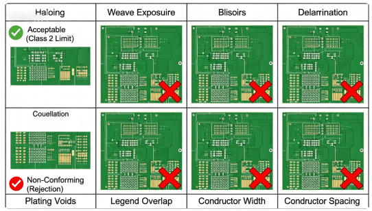
Quality Control Checklist
| Inspection Stage | Tests Performed | Acceptance Criteria |
|---|---|---|
| Preproduction | Material inspection (thickness, composition), phototool verification | Meets IPC-4201 (flexible base materials) and client specifications |
| After Etching | AOI (trace width, spacing, shorts, opens), copper thickness measurement | Trace width tolerance ±10%, no shorts/opens, copper thickness within 5% of target |
| After Lamination | Dimensional accuracy, layer alignment, bond strength test | Alignment tolerance ±0.1mm, bond strength ≥1.5N/mm |
| Final Inspection | Electrical testing (continuity, insulation resistance, impedance), X-ray (for vias), visual inspection | Continuity 100%, insulation resistance ≥100MΩ, impedance within ±10% of target |
Flexible PCB Cost & FAQs
Cost of Flexible PCB Manufacturing
| Cost Factor | Impact on Pricing |
|---|---|
| Number of Layers | Multilayer flex PCBs (3+ layers) cost more than single/double-sided due to complexity. |
| Material Type | Polyimide (Kapton) is more expensive than PET; high-temperature polyimide (e.g., Upilex) adds cost. |
| Copper Thickness | Thicker copper (≥2oz) increases material and fabrication costs. |
| Surface Finish | Immersion gold is costlier than OSP or immersion tin. |
| Volume | High-volume production (10,000+ units) reduces per-unit cost via economies of scale. |
| Lead Time | Expedited delivery (24–48 hours) adds a premium. |
As a ballpark, a simple single-sided flex PCB prototype (10 units) starts at $150–$300, while a complex multilayer rigid-flex PCB for automotive use can exceed $1,000 for a small batch.
Frequently Asked Questions (FAQs)
What is the minimum order quantity (MOQ) for flexible PCBs?
We have no strict MOQ—we can produce 1 prototype or 100,000+ units based on your needs.
How long does flexible PCB fabrication take?
Prototypes: 5–7 business days.
Small batches (10–100 units): 7–10 business days.
Mass production: 10–15 business days (plus material lead times for rare components).
Can you source components for flex PCB assembly?
Yes. Our component sourcing team procures active/passive components from authorized distributors (Digi-Key, Mouser, etc.) and can handle obsolete parts or custom components.
What file formats do you accept for flexible PCB design?
We accept Gerber files (RS-274X), BOMs (Excel/CSV), and pick-and-place files. We work with Altium, KiCad, and other major CAD tools.
Do you offer design services for flexible PCBs?
While our core strength is manufacturing, we provide DFM reviews and can recommend design improvements. For full PCB design, we partner with specialized firms.
What warranty do you offer on flexible PCBs?
We offer a 30-day warranty against manufacturing defects. If an issue arises from our process, we’ll repair or replace the PCBs at no cost.