Teflon PCB Manufacturer
High-Frequency PTFE PCB Solutions for Extreme Environments by HCJMPCBA
1. Introduction to Teflon PCB
- Ultra-low dielectric loss for high-frequency signal integrity.
- Extreme temperature resilience (-200°C to 260°C continuous operation).
- Chemical inertness against acids, bases, and solvents.
2. Core Advantages of Teflon PCB
The technical superiority of Teflon PCBs stems from PTFE’s material science. Below is a data-driven breakdown of their key benefits:
| Advantage | Technical Specification | Business Impact |
|---|---|---|
| Ultra-Low Dielectric Loss | DF ≤ 0.001 @ 10GHz (varies by PTFE grade) | Enables 5G/6G mmWave (28–77GHz) and satellite communications with minimal signal attenuation. |
| Stable Dielectric Constant | DK = 2.1–2.3 (deviation ±0.02 across temperature/frequency) | Ensures consistent impedance control (50Ω/75Ω) for high-speed digital and RF designs. |
| Extreme Temperature Tolerance | -200°C to 260°C continuous operation; short-term up to 300°C | Suitable for aerospace (cryogenic environments) and medical (autoclave sterilization) applications. |
| Ultra-Low Moisture Absorption | Moisture absorption < 0.01% (compliant with IPC-4101 Class H) | Guarantees long-term reliability in humid or outdoor environments (e.g., 5G base stations). |
| Chemical Inertness | Resistant to acids, bases, solvents, and most industrial chemicals | Ideal for industrial sensors and marine electronics exposed to corrosive substances. |
3. Teflon PCB Material Types & Specifications
PTFE-based laminates vary by filler, thickness, and performance. Below is a comparison of mainstream Teflon PCB materials:
| PTFE Grade | Dielectric Constant (DK) @ 10GHz | Dielectric Loss (DF) @ 10GHz | Thickness Range (mm) | Key Features | Typical Applications |
|---|---|---|---|---|---|
| Dupont Teflon™ AF | 2.1 ± 0.02 | 0.0009 | 0.025–1.5 | Fluorinated ethylene propylene (FEP) filler, ultra-low loss, flexible | 60GHz mmWave antennas, high-speed digital backplanes |
| Dupont Teflon™ F4B | 2.2 ± 0.02 | 0.001 | 0.1–3.0 | Glass fiber reinforcement, rigid, cost-effective | 5G base station RF modules, automotive radar |
| Domestic Modified PTFE (HCJMPCBA Custom Grade) | 2.2 ± 0.03 | 0.001 | 0.1–2.0 | Ceramic filler, 30% cost reduction vs. imported grades | Industrial RF sensors, mid-range wireless systems |
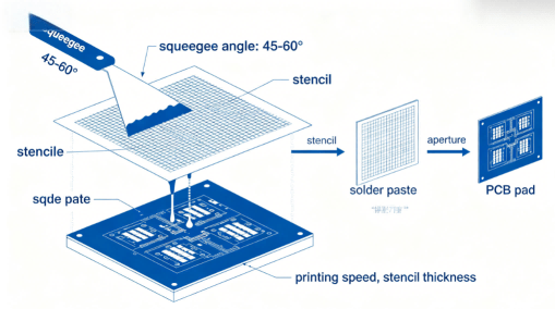
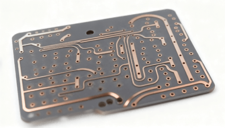
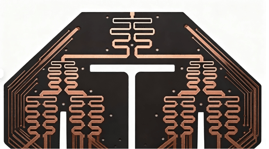
4. Teflon PCB Manufacturing Process
Step 1: Lamination
- Parameters:
- Temperature: 300–380°C (varies by PTFE grade; e.g., Teflon™ AF requires 350°C).
- Pressure: 50–100 bar.
- Hold Time: 60–120 minutes to ensure complete curing and void-free bonding.
- Challenge: Maintaining uniform pressure across the panel to prevent delamination, especially for multi-layer stacks.
Step 2: Drilling
- Methods:
- Laser Drilling: Minimum hole diameter 0.1mm, positional accuracy ±0.01mm, hole wall roughness Ra ≤ 0.5μm.
- Mechanical Drilling: For larger holes (≥0.3mm), using carbide drills with TiAlN coating to withstand PTFE’s abrasiveness.
- Inspection: Post-drilling AOI (Automated Optical Inspection) to verify hole size, location, and absence of debris.
Step 3: Plating & Surface Finish
- Plating: Copper thickness 1–3oz, with electroplating current density 2–4 A/dm² for uniform coverage.
- Surface Finish Options:
- ENIG (Electroless Nickel Immersion Gold): ≥0.05μm gold thickness for wire bonding and high-reliability applications.
- Hard Gold Plating: 0.5–2.0μm gold thickness for wear-resistant contacts (e.g., switches, connectors).
- OSP (Organic Solderability Preservative): Cost-effective for short-term storage in controlled environments.
Step 4: Testing & Validation
- Electrical Testing: TDR (Time Domain Reflectometry) for impedance control (±5% tolerance) and flying probe for 100% continuity.
- Thermal Testing: Thermal cycling (-200°C to +260°C, 500 cycles) to validate long-term reliability.
- X-Ray Inspection: Verifies via integrity and copper thickness uniformity.
5G & mmWave Communications
- Solution: Teflon™ AF PCB (DK=2.1, DF=0.0009) for 77GHz automotive radar modules.
- Outcome: Supports 77GHz frequency band with 40% lower signal loss than FR4, enabling 300m detection range for autonomous vehicles.
Medical Devices
- Solution: Teflon™ F4B PCB for autoclave-sterilized surgical tools.
- Outcome: Withstands 260°C steam sterilization cycles, meets ISO 10993 biocompatibility standards, and maintains electrical performance over 5,000 sterilization cycles.
Aerospace & Defense
- Solution: Custom modified PTFE PCB for satellite payloads.
- Outcome: Operates in -200°C cryogenic environments with dimensional stability ≤0.05%, ensuring 10-year mission reliability.
Industrial RF Systems
- Solution: Domestic modified PTFE PCB for industrial IoT sensors.
- Outcome: Resists harsh chemicals (acids, solvents) in manufacturing plants, with a 50% longer lifespan than FR4-based sensors.
6. Teflon PCB Design Guidelines: HCJMPCBA’s Expert Checklist
To maximize performance and manufacturability, follow these guidelines:
| Design Aspect | Best Practice | Rationale |
|---|---|---|
| Impedance Control | Target 50Ω (single-ended) / 100Ω (differential), account for DK deviation ±0.02 | Ensures signal integrity for RF and high-speed digital applications. |
| Trace Routing | Trace width ≥0.15mm, spacing ≥0.15mm; use curved traces (avoid 90° bends) | Minimizes signal reflection and crosstalk in high-frequency designs. |
| Thermal Management | Place 2–3 thermal vias (0.3mm diameter, copper-filled) per cm² under power components | Efficiently dissipates heat, preventing component overheating in high-power RF modules. |
| Mechanical Reliability | Maintain ≥0.5mm copper edge clearance; use stiffeners for flexible PTFE grades | Prevents copper cracking and board warpage during assembly and operation. |
7. HCJMPCBA’s Teflon PCB Manufacturing Capabilities
As a leading Teflon PCB manufacturer, HCJMPCBA delivers industry-leading precision and flexibility:
| Capability | Technical Specification | Business Benefit |
|---|---|---|
| Material Coverage | Dupont Teflon™ AF, F4B, and domestic modified PTFE grades | Supports diverse applications from 5G to aerospace. |
| Manufacturing Precision | Layer alignment tolerance ±0.02mm, impedance control ±5% | Ensures consistent signal integrity for high-frequency designs. |
| Quality Certifications | ISO 9001, AS9100 (aerospace), ISO 13485 (medical), RoHS | Qualifies for regulated industries (automotive, medical, aerospace). |
| Turnaround Time | Prototypes: 3–5 days; Mass production: 7–10 days | Accelerates product development cycles. |
| Global Sourcing & Delivery | Direct sourcing from Dupont and domestic suppliers; delivery to North America, Europe, Asia | Minimizes lead time and supports global supply chains. |
8. In-Depth FAQs About Teflon PCB
1. How to select the right PTFE laminate for 77GHz automotive radar?
For 77GHz, prioritize Dupont Teflon™ AF (DK=2.1, DF=0.0009) due to its ultra-low loss and FEP filler, which minimizes signal attenuation in mmWave bands. Ensure the laminate thickness (e.g., 0.127mm) aligns with your impedance and mechanical requirements.
2. What are the common defects in Teflon PCB lamination and how to solve them?
Delamination: Caused by insufficient pressure or temperature. Solution: Verify lamination parameters (350°C, 80 bar for Teflon™ AF) and use vacuum-assisted lamination.
Voids: Caused by trapped air. Solution: Pre-bake PTFE sheets at 125°C for 4 hours to remove moisture before lamination.
3. How to control the cost of small-batch Teflon PCB production?
Opt for domestic modified PTFE grades (30% cost reduction vs. imported Dupont grades).
Use standard panel sizes (e.g., 18″×24″) to minimize material waste.
Leverage HCJMPCBA’s prototype-friendly pricing for orders ≥5 pieces.
4. Does Teflon PCB meet FDA/USP Class VI certification for medical devices?
Yes. Teflon™ F4B and select modified PTFE grades meet FDA 21 CFR 177.1550 and USP Class VI standards, making them suitable for implantable and sterile medical devices.
5. Teflon PCB vs Rogers PCB: Which is better for 5G applications?
Teflon PCB (PTFE): Ideal for 28–77GHz mmWave (DF≤0.001, stable DK), extreme temperatures, and chemical resistance.
Rogers PCB (PTFE-based with ceramic filler): Better for 5–28GHz (higher DK options, lower cost for mid-frequency).
Choose Teflon for mmWave and extreme environments; Rogers for mid-frequency 5G applications.
6. How to ensure long-term reliability of Teflon PCB in harsh environments?
Implement gold plating (≥0.05μm) for corrosion resistance.
Use thermal vias (0.3mm diameter, copper-filled) for heat dissipation.
Design with edge copper clearance ≥0.5mm to prevent mechanical stress.
HCJMPCBA combines Teflon’s material innovation with our precision manufacturing expertise to deliver PCBs that meet the most demanding technical requirements. Whether you’re developing a 5G base station, automotive radar, or aerospace component, our team of engineers provides end-to-end support—from design review to mass production.