PCB Assembly FAQs
Expert Answers for Buyers & Engineers - HCJMPCBA
Q1: What is PCB Assembly (PCBA)?
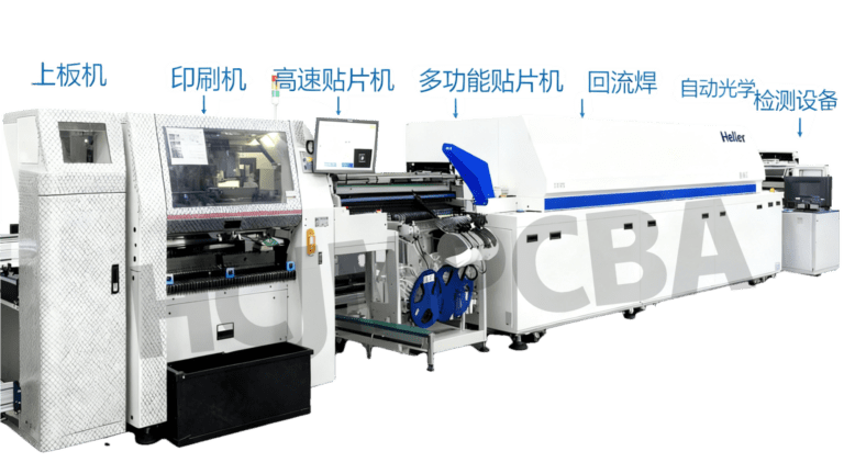
Answer: PCB Assembly (PCBA) is the process of mounting electronic components (surface-mount/SMT or through-hole/THT) onto a bare PCB to form a functional electronic circuit. The core workflow follows 5 key steps:
Q2: What’s the Difference Between SMT and Through-Hole Assembly? How to Choose?
Answer: The choice depends on component type, application requirements, and production volume. Below is a detailed comparison:
| Comparison Aspect | SMT Assembly | Through-Hole Assembly |
|---|---|---|
| Component Type | Small, lightweight (01005~50mm×50mm), surface-mount pads (e.g., resistors, ICs) | Larger, high-power (e.g., connectors, electrolytic capacitors), through-hole pins |
| Placement Method | Automated pick-and-place machines (speed: up to 50,000 components/hour) | Manual insertion or automated equipment + wave soldering |
| Key Advantages | High component density, low cost for mass production, compact design | Strong mechanical stability, high current-carrying capacity, durable for vibration |
| Ideal Applications | Consumer electronics (smartphones, routers), 5G modules, compact devices | Industrial control, automotive electronics, aerospace equipment |
How to Choose:
- Use SMT for miniaturized, high-volume designs (e.g., 10,000+ units) to save space and cost.
- Use through-hole for power components or connectors requiring mechanical strength (e.g., automotive wiring harnesses).
- Hybrid assembly (SMT + through-hole) is common for complex devices (e.g., industrial PLCs).
Q3: What Files Are Required for PCBA? What Format Standards Must Be Followed?
Answer: Three mandatory files are required to ensure error-free production; optional documents help optimize processes:
| File Type | Format | Mandatory Content | Accuracy Requirement |
|---|---|---|---|
| Gerber Files | RS-274X (Extended Gerber) | Copper layers (top/bottom/inner), solder mask, silkscreen, board outline, solder paste layers | 3.6 coordinate format (3 integers + 6 decimals), consistent units (mm recommended) |
| BOM (Bill of Materials) | Excel (.xls/.xlsx) or CSV | Reference designator (R1, C2), MPN, package, quantity, polarity, tolerance | Part number matching rate 100%, no duplicate reference designators |
| Centroid File | XYRS (X/Y coordinates, rotation, side) | Reference designator, X/Y coordinates, rotation angle (0–360°), board side (Top/Bottom) | ±0.02mm coordinate accuracy, rotation error ≤1° |
- Assembly drawings (highlight critical requirements: component height limits, thermal pads).
- Test point lists (for functional testing) and physical samples (for prototype validation).
Q4: How to Avoid File-Related Delays in Production?
- Use HCJMPCBA’s free DFM (Design for Manufacturability) check tool (available on our portal) to validate files within 6 hours—we’ll flag missing layers, incorrect units, or incompatible formats.
- Follow naming conventions: e.g., “ProjectName_TopCopper.gtl” “ProjectName_BOM.xlsx” (avoid special characters).
- Double-check for common errors:
- Gerber files: Ensure no missing solder mask/silkscreen layers.
- BOM: Verify polarity for diodes/ICs (mark “+/-” or “Pin 1”).
- Centroid file: Align coordinates with Gerber (use the same origin point).
- Submit files 24 hours before production to allow for revisions (if needed).
Q5: What Factors Affect PCBA Cost? How to Reduce Costs Without Sacrificing Quality?
Key Cost Drivers:
| Cost Factor | Impact on Cost | Example |
|---|---|---|
| Order Volume | Setup fee ($8–$12) is fixed; bulk orders reduce per-unit cost | 10pcs: $5/piece; 1000pcs: $1.2/piece |
| Component Complexity | 01005 components cost 20% more than 0402; fine-pitch BGA adds $0.005–$0.01 per joint | 200 joints with 01005 components: $0.4; with 0402: $0.32 |
| Testing Requirements | FCT (Functional Test) costs 2–3x more than AOI | AOI: $0.5/piece; FCT: $1.5/piece |
Cost-Saving Strategies (How to Reduce Costs):
- Design Optimization:
- Panelize small PCBs (≤50×100mm) into 250×250mm panels to share setup fees (e.g., 6×10cm PCBs per panel = 60% cost reduction per unit).
- Avoid blind/buried vias (add $0.1–$0.3 per via) and use standard vias (0.3mm diameter).
- Component Selection:
- Use domestic alternatives (e.g., Chinese MLCCs vs. Japanese) for non-critical applications (30% cost reduction).
- Choose in-stock components (HCJMPCBA’s 40k+ inventory) to avoid sourcing delays and premium fees.
- Process Simplification:
- Use automated SMT instead of manual assembly (30% labor cost reduction).
- Skip FCT for prototypes; use AOI + flying probe tests (covers 99% of defects).
Q6: What Is the Typical Lead Time for PCBA? How to Handle Rush Orders?
Standard Lead Time:
| Order Type | Quantity | Lead Time | Included Services |
|---|---|---|---|
| Prototype | 1–50pcs | 3–5 days | PCB fabrication + SMT assembly + AOI/X-ray inspection |
| Mass Production | 500–10,000pcs | 7–12 days | Full QC (SPI + AOI + FCT) + packaging + global shipping |
Rush Service (24–48h Delivery):
- Eligibility: Prototypes (1–50pcs) with complete, error-free files and in-stock components.
- Cost: 30–50% premium on standard pricing (varies by order size).
- How to Qualify:
- Submit files via our “Rush Order” portal (www.hcjm-pcba.com/RFQ).
- Confirm component availability with our sales team (24/7 support).
- Accept simplified testing (AOI + flying probe instead of FCT).
Answer: Our state-of-the-art equipment supports high-precision and high-volume production:
| Capability | Technical Specification | Application Scenario |
|---|---|---|
| Placement Accuracy | ±0.01mm (high-precision machines: Fuji NXT III) / ±0.025mm (high-speed machines: Yamaha YSM40R) | Fine-pitch BGA (0.4mm pitch), QFN packages |
| Component Range | SMT: 01005 (0.4mm×0.2mm) to 50mm×50mm; through-hole: wire diameter 0.4–2.0mm | Consumer electronics, industrial control, automotive |
| 贴装 Speed | Up to 50,000 components/hour (high-speed lines) / 30,000 components/hour (high-precision lines) | Mass production (e.g., 100k+ units/month) |
Q8: What Soldering Processes Are Used? What Are the Key Parameters for Reliability?
Answer: We use two core soldering processes, optimized for different component types:
| Process | Equipment | Key Parameters | Quality Standard |
|---|---|---|---|
| Reflow Soldering (SMT) | Heller 1809EXL (8 温区) | Peak temperature: 245±5°C; preheat: 150–180°C (60s); nitrogen purity: 99.99% | IPC-J-STD-001 Class II/III |
| Wave Soldering (Through-Hole) | ERSA Versaflow 3/45 | Wave temperature: 255±5°C; preheat: 150–180°C; flux residue: <0.1mg/in² | IPC-J-STD-001 Class II |
- Use lead-free solder paste (Sn96.5Ag3.0Cu0.5) compliant with RoHS 2.0.
- For high-reliability applications (e.g., aerospace), use nitrogen reflow to reduce oxidation.
- Conduct SPI (Solder Paste Inspection) to ensure paste thickness (0.10–0.15mm) and uniformity.
Q9: What Quality Control (QC) Processes Are in Place for PCBA?
Answer: We follow a 4-stage QC workflow to ensure 99.8% first-pass yield:
| QC Stage | Inspection Method | Key Checkpoints | Acceptance Criteria |
|---|---|---|---|
| Incoming Material Inspection | Visual inspection + solderability test | PCB warpage, component oxidation, BOM matching | PCB warpage ≤0.75%, component solderability ≥95% |
| In-Process Inspection | SPI (solder paste) + AOI (placement) | Paste thickness, component alignment, polarity | Paste thickness variation ±10%, 0 polarity errors |
| Post-Soldering Inspection | AOI + X-ray (BGA/QFN) | Soldering defects (voids, bridging), hidden joints | BGA voids ≤25% (IPC-7095), 0 critical defects |
| Final Testing | ICT (continuity) + FCT (functionality) | Electrical continuity, functional performance | 100% continuity, functional yield ≥99.5% |
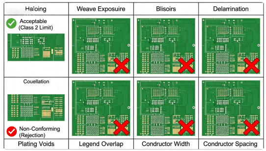
Q10: What Are Common PCBA Defects? How to Prevent & Resolve Them?
Answer: The most frequent defects (and solutions) are:
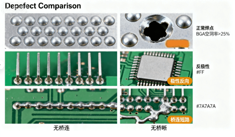
| Defect Type | Root Cause | Prevention (How to Avoid) | Resolution (How to Fix) |
|---|---|---|---|
| BGA Voids | Flux volatilization, preheat too fast, PCB moisture | Use low-void solder paste; pre-bake PCBs (125°C/4h); extend preheat to 60–90s | Vacuum reflow (10–20 mbar); rework with hot air station |
| Bridging (Short Circuits) | Excess solder paste, stencil aperture too large | Optimize stencil aperture (80% of pad width); reduce paste thickness | Remove excess solder with 0.2mm soldering iron tip |
| Polarity Reversal | Incorrect Centroid file, missing polarity marks | Add polarity marks in Gerber; double-check Centroid rotation | Rework with hot air station; replace damaged components |
Q11: What Industry Standards Does HCJMPCBA Comply With? How to Ensure Compliance for My Application?
Answer: We meet global standards for key industries; compliance is tailored to your use case:
| Industry | Compliance Standards | Special Requirements |
|---|---|---|
| Consumer Electronics | RoHS 2.0, CE, FCC | Lead-free components, EMI shielding (if needed) |
| Medical Devices | ISO 13485, FDA 21 CFR Part 820, IPC-A-610 Class III | Biocompatible materials, 100% FCT testing |
| Automotive | IATF 16949, AEC-Q100, ISO 16750 | Wide temperature range (-40°C to +125°C), vibration resistance |
| Aerospace | AS9100, MIL-STD-202G | High-reliability components, burn-in testing (125°C/48h) |
- Inform our sales team of your target industry (e.g., “medical device”) during quoting.
- Provide compliance requirements (e.g., “ISO 13485”) and we’ll adjust processes (e.g., Class III inspection).
- Request a compliance report (included with bulk orders) with test data and certification copies.
Q12: Can HCJMPCBA Support Customized PCBA for Special Applications (e.g., High-Temp, High-Power)?
- High-Temperature Applications (e.g., industrial furnaces): Use ceramic substrates (AlN, thermal conductivity ≥170W/m·K) or high-Tg FR4 (Tg≥170°C), operating temperature up to 150°C.
- High-Power Applications (e.g., EV controllers): Implement copper pillar heat sinks (thermal resistance ≤0.2°C/W) and thermal vias (2–3 vias/cm²).
- High-Frequency Applications (e.g., 5G base stations): Use low-loss substrates (Teflon/PTFE) and impedance control (±5% tolerance).
- Share your application requirements (temperature range, power density, frequency) via email.
- Provide design files and our engineering team will propose optimized solutions (e.g., substrate selection, thermal management).
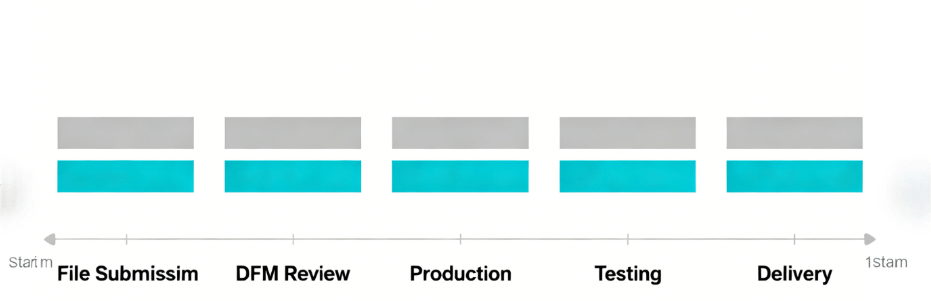
Q13: What Is the Order Process for PCBA? How to Track Production Progress?
- File Submission: Upload Gerber, BOM, and Centroid files via our portal (www.hcjm-pcba.com/upload).
- DFM Review: Our engineers complete analysis within 6 hours and provide optimization suggestions.
- Quotation Confirmation: Receive a detailed quote (cost breakdown + lead time) and confirm the order.
- Production: Track progress in real time via our online system (see screenshot below).
- Delivery: Test reports (AOI/X-ray/FCT) are sent with the order; global shipping (DHL/FedEx) is available.
Q14: What After-Sales Support Is Provided? What Is the Warranty Policy?
- Warranty: 90-day warranty for all PCBA products. We offer free rework/replacement for defects caused by our process (e.g., soldering errors, component misplacement).
- Technical Support: 24/7 engineering support for post-delivery issues (e.g., functional failures, defect analysis).
- Return Policy: Accept returns within 7 days of delivery for non-customized orders (unused, unmodified).
- Contact our after-sales team (aftersales@hcjm-pcba.com) with your order number and defect photos/videos.
- We’ll conduct a root cause analysis within 48 hours and propose a solution (rework, replacement, or refund).