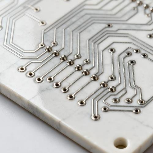
Ceramic PCB
Ceramic PCB Technology
HCJMPCBA’s Advanced Solutions for High-Temp & High-Power Electronics
1. Introduction to Ceramic PCB
A Ceramic PCB (ceramic printed circuit board) is a revolutionary electronics substrate fabricated from advanced ceramic materials—including alumina (Al₂O₃), aluminum nitride (AlN), and silicon nitride (Si₃N₄). These materials deliver unmatched performance in three core areas:
- Ultra-High Thermal Conductivity: Up to 300 W/m·K (compared to FR4’s 0.3 W/m·K), enabling efficient heat dissipation in high-power devices .
- Extreme Temperature Resistance: Sustains continuous operation above 1000°C and short-term thermal shocks up to 1500°C .
- Electrical Insulation & Mechanical Strength: Provides dielectric strength >10 kV/mm and flexural strength up to 1000 MPa, making it ideal for harsh environments.
As a leading ceramic PCB manufacturer, HCJMPCBA leverages these properties to serve industries like power electronics, aerospace, automotive, and LED lighting. Our high thermal conductivity ceramic circuit boards enable designs that were once impractical with traditional FR4 or metal-core PCBs.
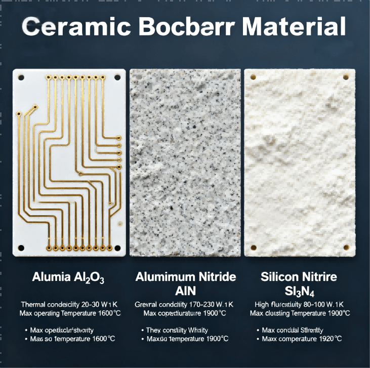
2. Ceramic PCB Material Types & Specifications
Ceramic PCBs are categorized by their base material, each optimized for specific performance needs. The table below compares the most widely used ceramic substrates:
| Material | Thermal Conductivity (W/m·K) | Dielectric Constant (DK) | Max Operating Temperature (°C) | Flexural Strength (MPa) | Typical Applications |
|---|---|---|---|---|---|
| Alumina (Al₂O₃) | 20–30 | 9.8 | 1600 | 250–350 | LED substrates, general power modules, automotive sensors |
| Aluminum Nitride (AlN) | 170–230 | 8.8 | 1900 | 400–500 | 5G base station power amplifiers, EV motor controllers, high-power LEDs |
| Silicon Nitride (Si₃N₄) | 80–100 | 7.8 | 1900 | 800–1000 | Aerospace engine sensors, industrial high-temperature furnaces, nuclear electronics |
HCJMPCBA specializes in three leading ceramic PCB fabrication technologies, each with unique advantages:
Direct Plating Copper (DPC)
DPC is ideal for high-precision, high-power applications:
- Process Steps:
- Photolithography: Define copper traces with line width/spacing ≥50μm.
- Electroplating: Deposit copper (10–100μm thick) onto the ceramic substrate.
- Sintering: Heat at 400–600°C to ensure copper adhesion ≥10N/cm .
- Key Advantages: High conductivity, fine feature resolution, and compatibility with SMT assembly.
- Applications: 5G RF modules, laser diodes, and medical devices.
High-Temperature Co-Fired Ceramic (HTCC)
HTCC enables complex, multi-layer ceramic circuits:
- Process Steps:
- Green Tape Punching: Create vias in ceramic green sheets (0.1–0.5mm thick).
- Conductive Paste Filling: Fill vias with tungsten or molybdenum paste.
- Lamination & Co-Firing: Stack sheets and fire at 1500–1700°C, achieving dimensional accuracy ±0.1mm .
- Key Advantages: High integration, hermetic sealing, and extreme temperature resistance.
- Applications: Aerospace avionics, military radars, and high-reliability sensors.
Low-Temperature Co-Fired Ceramic (LTCC)
LTCC balances performance and cost for mid-power applications:
- Process Steps:
- Green Tape Processing: Cut, punch, and print on ceramic green sheets.
- Lamination: Stack sheets under pressure (10–20 MPa).
- Co-Firing: Fire at 850–950°C, with dielectric constant deviation ±0.05 .
- Key Advantages: Lower cost than HTCC, compatible with silver and gold conductors.
- Applications: Automotive infotainment, IoT sensors, and consumer electronics.
4. Technical Advantages of Ceramic PCB
Ceramic PCBs outperform traditional substrates in five critical areas, as shown in the table below:
| Performance Metric | Ceramic PCB (AlN Example) | FR4 PCB | MCPCB (Metal-Core PCB) |
|---|---|---|---|
| Thermal Conductivity | 170–230 W/m·K | 0.3 W/m·K | 1–20 W/m·K (aluminum core) |
| Operating Temperature | -200°C to 1000°C+ | -55°C to 130°C | -55°C to 150°C |
| Dielectric Strength | >10 kV/mm | 1–2 kV/mm | 1–3 kV/mm |
| Coefficient of Thermal Expansion (CTE) | 4.5–7 ppm/°C (matches silicon) | 14–18 ppm/°C | 12–23 ppm/°C (aluminum core) |
| Chemical Resistance | Resists acids, bases, and solvents | Susceptible to moisture and chemicals | Aluminum core prone to corrosion |
5. Application Cases (Industry-Specific)
Ceramic PCBs enable breakthroughs in industries with extreme performance demands:
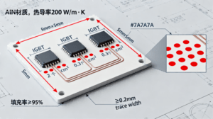
Power Electronics (EV & Industrial)
- Solution: AlN PCB (thermal conductivity 200 W/m·K) for an electric vehicle’s IGBT module.
- Outcome: Power density increased by 50%, junction temperature reduced by 25°C, and component lifespan extended by 3x compared to FR4-based designs .
LED Lighting
- Solution: Al₂O₃ PCB (thermal conductivity 25 W/m·K) for COB (Chip-on-Board) LED fixtures.
- Outcome: Luminous efficacy improved by 30%, and operating life extended to 100,000 hours—critical for commercial and industrial lighting applications .
Aerospace & Defense
- Solution: Si₃N₄ PCB (operating temperature 1200°C) for an aerospace engine sensor.
- Outcome: Withstood vibration (20–2000 Hz, 10g acceleration) and thermal shocks, achieving 40% higher reliability than metal-core alternatives .
5G Communications
- Solution: AlN DPC PCB for a 5G base station’s power amplifier module.
- Outcome: Supported 28 GHz mmWave frequencies with 20% lower insertion loss, enabling wider coverage and faster data speeds .
6. Ceramic PCB Design Guidelines: HCJMPCBA’s Expert Checklist
| Design Aspect | Best Practice | Rationale |
|---|---|---|
| Thermal Management | Place ≥2 thermal vias (0.3mm diameter, copper-filled) per cm² under power components | Efficiently dissipates heat, preventing component overheating in high-power applications. |
| Component Placement | Maintain ≥5mm clearance between power components and ceramic substrate edges | Reduces thermal stress and prevents substrate cracking. |
| Solder Selection | Use SnAgCu solder (CTE ≈22 ppm/°C) to match ceramic’s thermal expansion | Minimizes thermal cycling fatigue and solder joint failure. |
| Trace Routing | Use gradual curves instead of 90° bends; maintain trace width ≥0.2mm | Reduces signal reflection and ensures sufficient current-carrying capacity. |
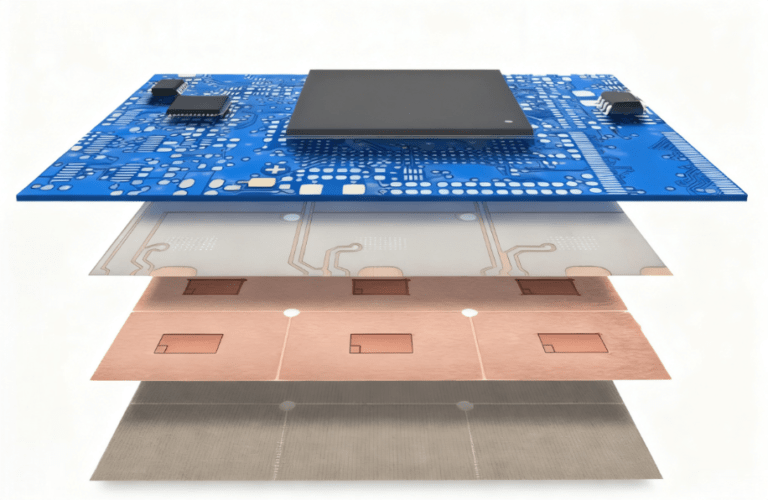
7. HCJMPCBA’s Ceramic PCB Manufacturing Capabilities
As a premier ceramic PCB supplier, HCJMPCBA offers industry-leading capabilities:
| Capability | Technical Specification | Business Benefit |
|---|---|---|
| Material Coverage | Al₂O₃, AlN, Si₃N₄, and custom ceramic formulations | Supports diverse applications from consumer electronics to aerospace. |
| Manufacturing Processes | DPC, HTCC, LTCC, and hybrid processes | Enables tailored solutions for cost, precision, and performance. |
| Precision & Quality | DPC line width/spacing ≥50μm; HTCC dimensional accuracy ±0.05mm | Ensures reliability in high-precision applications like 5G and medical devices. |
| Certifications | ISO 9001, IATF 16949 (automotive), AS9100 (aerospace), ISO 13485 (medical) | Qualifies for regulated industries with strict quality requirements. |
| Turnaround Time | Prototypes: 5–7 days; Mass production: 10–15 days | Accelerates product development cycles. |
| Global Delivery | North America, Europe, Asia, and beyond | Supports global supply chains and just-in-time manufacturing. |
8. In-Depth FAQs About Ceramic PCB
1. How to choose between Al₂O₃, AlN, and Si₃N₄ ceramic PCBs for power electronics?
- Al₂O₃: Best for cost-sensitive applications (e.g., general power modules, LED substrates) where thermal conductivity ≥20 W/m·K is sufficient.
- AlN: Ideal for high-power devices (e.g., EV motor controllers, 5G power amplifiers) requiring thermal conductivity ≥170 W/m·K and CTE matching silicon (4.5 ppm/°C).
- Si₃N₄: Suited for extreme environments (e.g., aerospace engines, industrial furnaces) needing thermal shock resistance and flexural strength >800 MPa .
2. DPC vs HTCC vs LTCC: Which ceramic PCB process is best for my application?
- DPC: Choose for high-precision, high-conductivity designs (e.g., 5G RF modules, laser diodes) where fine feature resolution (≥50μm) is critical.
- HTCC: Opt for complex, multi-layer circuits (e.g., aerospace avionics, military radars) requiring hermetic sealing and extreme temperature resistance.
- LTCC: Select for mid-power, cost-effective applications (e.g., automotive infotainment, IoT sensors) where silver/gold conductors and lower firing temperatures (850–950°C) reduce costs .
3. What’s the cost difference between ceramic PCB and FR4 for high-power designs?
Ceramic PCBs cost 2–5x more than FR4, but they reduce overall system cost by:
- Eliminating heat sinks (due to superior thermal conductivity).
- Increasing component lifespan (reduced thermal stress).
- Enabling smaller form factors (higher power density).For high-power applications (≥100W), the total cost of ownership for ceramic PCBs is often lower than FR4 over the product’s lifetime .
4. How to ensure long-term reliability of ceramic PCB in harsh environments?
- Material Selection: Choose Si₃N₄ for thermal shock resistance or AlN for chemical inertness.
- Surface Finish: Use ENIG (Electroless Nickel Immersion Gold) for corrosion resistance.
- Design: Implement thermal vias (0.3mm diameter, copper-filled) and maintain ≥5mm component-edge clearance.
- Testing: Subject boards to thermal cycling (-55°C to +150°C, 1000 cycles) and vibration testing (20–2000 Hz, 10g) .
5. Can ceramic PCBs be used for high-frequency (5G/6G) applications?
Yes. AlN and Si₃N₄ ceramic PCBs offer:
- Low dielectric loss (DF ≤0.002 at 10 GHz).
- Stable dielectric constant (DK = 8.8–7.8, deviation ±0.05).
- Controlled impedance (50Ω/75Ω) for mmWave frequencies (28–77 GHz).These properties make them ideal for 5G base stations, 6G R&D, and satellite communications .
6. What are the thermal management best practices for AlN PCB?
- Thermal Vias: Place 2–3 vias (0.3mm diameter, copper-filled) per cm² under power components.
- Heat Spreading: Use copper planes (≥2oz thickness) to spread heat evenly.
- Solder Paste: Apply thin solder paste (0.1–0.15mm thickness) to minimize thermal resistance.
- Component Attachment: Use sintered silver or gold-tin solder for low-thermal-resistance bonds .
Why Choose HCJMPCBA for Ceramic PCB?
HCJMPCBA combines ceramic material expertise with precision manufacturing to deliver PCBs that meet the most demanding technical requirements. Our capabilities span DPC, HTCC, and LTCC processes, with full support for Al₂O₃, AlN, and Si₃N₄ substrates. Whether you’re developing a 5G power amplifier, an EV motor controller, or an aerospace sensor, our team provides end-to-end support—from design review to mass production.


