What Is PCB Layout Design?
PCB layout design refers to converting schematics into a physical, manufacturable board with accurate footprint placement, stack-up planning, and routing. It involves establishing board outline, layer stack-up, trace routing, and rule settings such as clearance and impedance. This process bridges schematic capture and production-ready Gerber/BOM output.
Relevant terms include layout pcb, pcb design and layout, and design layout pcb.
Key Stages in PCB Layout Design
1. Defining Board Stack‑up & Design Rules
Start with fabrication partner’s DFM guidelines—track width, spacing, layer count, and impedance rules tailored to board complexity pcb board layout design. Early alignment prevents later manufacturing errors.
2. Component Placement Strategy
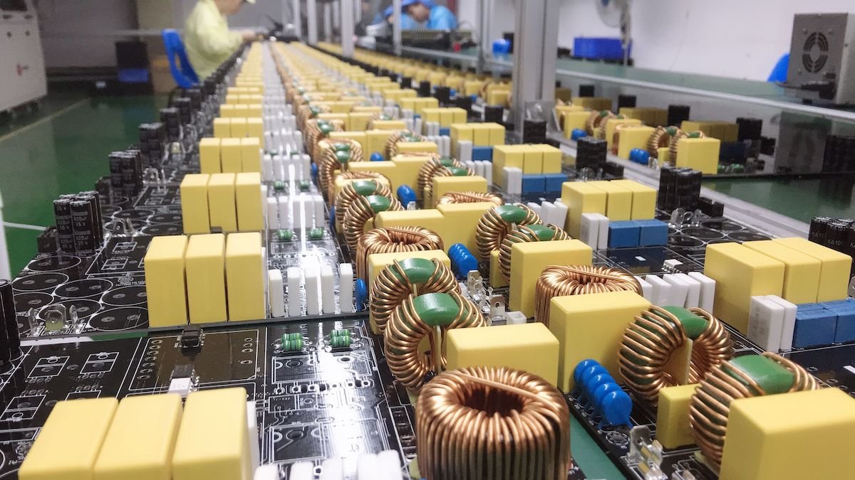
Place primary components (e.g. processors, power regulators) first. Group related parts and minimize via usage by reducing net crossings. It’s best to put all SMD components on one side for efficiency pcb board layout, pcb layouts.
3. Routing: Power, Ground & Signal Paths
Use continuous internal power and ground planes for stable return paths. Ensure trace widths match current load, and distribute high-current nets across multiple vias. Route high-speed signals over solid ground planes with gentle bends and avoid parallel coupling to reduce EMI and signal reflections pcb board layout pcb board layout software.
Advanced Layout Considerations for High‑Performance PCBs
Decoupling, EMI & Signal Integrity
Place decoupling capacitors close to IC pins and tie them to ground via short, low‑inductance paths. Isolate analog and digital sections to minimize crosstalk and noise. Manage differential pairs and impedance-controlled traces for reliability pcb layouts pcb layout schematic.
Design Rules Checking & Manufacturability
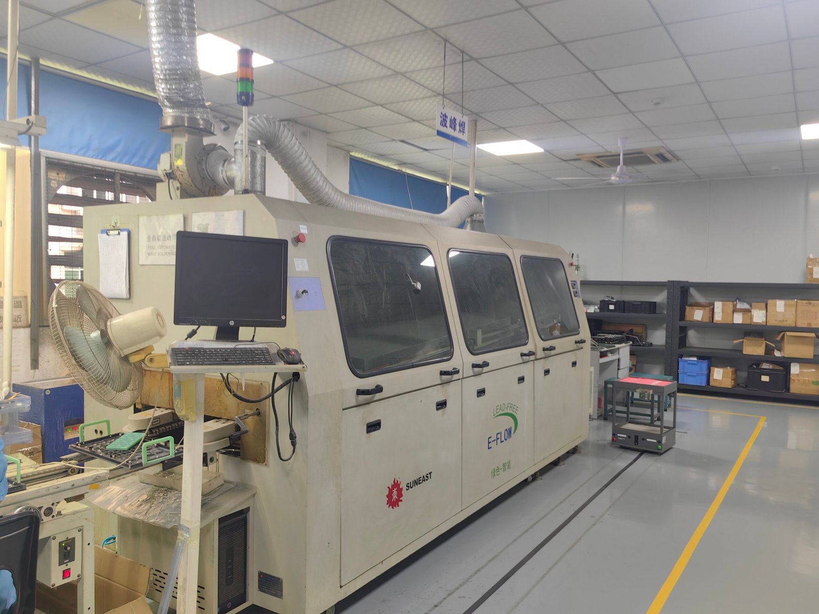
Run DRC checks frequently to verify trace spacing, net clearances, and silkscreen overlays. Add labels and logos in silkscreen layers. Ensure your layout meets DFM and PCB board layout guidelines to avoid errors during assembly.
Why Good PCB Layout Matters in PCBA Services
A quality pcb layout design improves first-pass yield, reduces assembly rework, and optimizes signal performance. At HCJMPCBA, our layouts are guided by strict SOPs ensuring compatibility with SMT processing, functional testing, and RF validation. For examples of high-speed and high-density designs, please view our case studies or explore HCJMPCBA’s SMT services.
How HCJMPCBA Ensures Layout Excellence
We use mainstream CAD tools (e.g. Altium, EasyEDA) for layout, adhering to best practices including stack-up setup, incremental DRC, routing strategy, and label overlays. We generate fabrication-ready Gerber files, BOM, and pick‑and‑place data. Advanced services include impedance simulation and layout review—especially critical for HDI or high-speed designs pcb design layout layout pcb simple pcb layout drawing.
How to Choose the Right PCB Layout Service
-
Prototype / Simple Layout: schematic-driven layout, single‑layer or minimal layers, manual route check.
-
High-Speed / HDI Layout: more layers, controlled impedance, consideration for EMI and manufacturability.
-
Advanced Layout Tools: require stack-up, DRC rules, simulation support (pcb board layout software, pcb board layout design, pcb layouts).
Choose vendors who ask for stack-up, DFM rules, and provide both layout review and output files.
Conclusion
Successful pcb layout design balances electrical integrity, manufacturability, and reliability. By following proven placement and routing practices, you ensure high-quality PCBs ready for assembly and certification. HCJMPCBA combines professional layout services with SMT assembly for seamless turnkey production.
To learn more PCBA services, please contact Guangzhou Huachuang Precision Technology (HCJMPCBA).