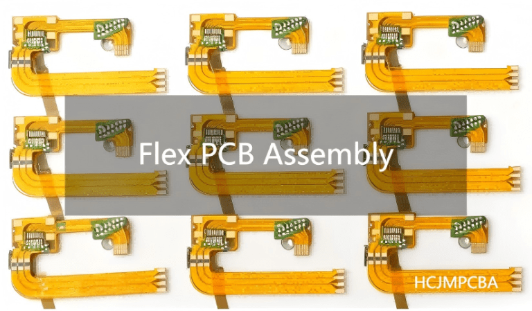
Flexible PCB Assembly
HCJMPCBA’s Precision Solutions for Advanced Electronics
Introduction: What is Flex PCB Assembly?
Differences Between Flex PCB Assembly and Rigid Assembly
The unique properties of flexible pcb boards demand specialized assembly processes distinct from rigid PCB manufacturing. Below is a detailed comparison:
| Aspect | Flex PCB Assembly | Rigid PCB Assembly |
|---|---|---|
| Base Material | Polyimide (PI), PET (flexible substrates) | FR4, CEM (rigid substrates) |
| Assembly Fixtures | Custom rigid carriers to prevent bending during soldering | Standard vacuum fixtures |
| Component Limitations | No heavy components on bend zones; requires stiffeners for large parts | No restrictions on component weight/location |
| Soldering Temperature | Lower peak temps (≤245°C) to protect flexible substrates | Higher peak temps (260°C+) for FR4 durability |
| Inspection Methods | 3D AOI + manual bend testing | 2D AOI + X-ray (for BGAs) |
| Key Application | Wearables, foldable phones, automotive sensors | Computers, industrial controllers |
| Connector Requirements | Specialized flex pcb connectors (e.g., board-to-board flex connectors) | Standard pin headers, USB connectors |
Design Considerations for Flex PCB Assembly
Successful flexible pcb assembly starts with optimized design. Below are critical guidelines to ensure manufacturability and performance:
| Design Aspect | Best Practices | Common Pitfalls to Avoid |
|---|---|---|
| Bend Zone Design | – Maintain bend radius ≥5x board thickness (single-layer) – ≥20x for multilayer flex pcbs – Use curved traces instead of right angles |
– Placing components on bend lines – Sharp 90° traces in flex areas |
| Component Placement | – Keep components ≥3mm from bend zones – Use SMDs (01005–1210 size) for compactness – Add stiffeners under BGAs/QFNs |
– Through-hole components on flexible sections – Uneven component distribution (causes warping) |
| Material Selection | – Polyimide pcb for high temp (≥250°C) – PET for low-cost consumer goods – 1oz copper for balance of flexibility/conductivity |
– Using FR4 in flex zones – Thin copper (≤0.5oz) for high-current paths |
| Connector Integration | – Specify flex connector pcb with locking mechanisms – Leave ≥2mm clearance around connector pads |
– Standard rigid connectors on flex sections – Insufficient pad size for flex connectors |
| Solder Mask & Coverlay | – Coverlay opening ≥0.6mm × 0.6mm – Solder mask bridge ≥0.1mm (green) – Align coverlay with bend axes |
– Coverlay overlapping solder pads – No coverlay on high-stress bend zones |
| Impedance Control | – Single-ended: 50Ω ±10% – Differential pairs: 100Ω ±10% – Use PI substrate for stable impedance |
– Ignoring impedance in high-speed flexible printed circuits – Inconsistent trace width in controlled-impedance paths |
Characteristics of Flex Board Assembly
HCJMPCBA’s flexible pcb assembly delivers unique attributes that set it apart in the industry:
| Characteristic | Detailed Description | Industry Impact |
|---|---|---|
| High Precision | Supports component placement down to 01005 size; trace/spacing ≥2mil ; positional accuracy ±0.01mm | Enables miniaturization of bendable circuit boards for wearables |
| Material Compatibility | Works with PI, PET, and polyimide flex pcb; compatible with all surface finishes (ENIG, OSP, immersion tin) | Flexibility to meet diverse application requirements (automotive/medical) |
| Environmental Resilience | Assemblies withstand -40°C to +125°C; resistant to moisture, vibration, and chemicals | Reliable performance in harsh industrial/aerospace environments |
| Hybrid Assembly Capability | Integrates rigid flex pcbs with both SMT and THT components; supports stiffener lamination (PI/FR4/aluminum) | Reduces assembly steps for complex devices (e.g., smartwatches) |
| Cost Efficiency | Eliminates wiring harnesses; reduces connector count; scalable for high-volume flex pcb fab | Lowers total cost of ownership for consumer electronics brands |
| Fast Prototyping | Turnaround time for pcb prototype assembly: 3–5 business days | Accelerates product development cycles for tech startups |

HCJMPCBA’s Flex PCB Assembly Features & Capabilities
Our state-of-the-art facility delivers industry-leading flexible pcb assembly services. Below is a comprehensive overview of our technical capabilities:
| Category | Capability | Technical Specifications |
|---|---|---|
| Board Types | Flexible PCB | 1–8 layers; PI/PET substrate; thickness 0.08–0.4mm |
| Rigid-Flex PCB | 2–16 layers; PI + FR4; bend radius ≥10x thickness | |
| Flexible HDI PCB | Microvias (4mil); trace/spacing 2mil/2mil | |
| Component Handling | SMT Components | 01005 to 50mm BGA; QFN, LGA, SOT, SOIC |
| Special Components | Flex pcb connectors, LEDs, sensors, batteries | |
| Manufacturing Parameters | Board Size | Min: 6×6mm; Max: 800×240mm (2-layer) |
| Copper Thickness | 0.5oz–2oz (17.5μm–70μm) | |
| Surface Finish | ENIG, OSP, immersion tin, chemical silver | |
| Production Capacity | Order Volume | 1 piece (prototype) – 1,000,000+ pieces |
| Lead Time | 3–5 days (prototype); 7–14 days (mass production) | |
| Quality & Compliance | Standards | IPC-A-610, ISO 9001, RoHS, REACH |
| Testing Certifications | AEC-Q200 (automotive), IEC 60601 (medical) | |
| Value-Added Services | Engineering Support | DFM analysis, flexible pcb design optimization, component sourcing |
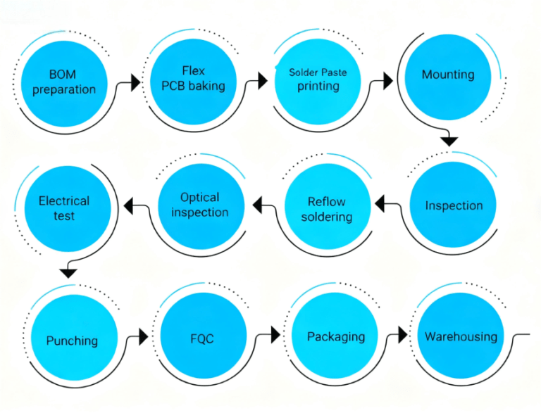
HCJMPCBA Flexible Printed Circuit Board Assembly [Step by Step]
Step 1: Design Review & DFM Analysis
- Receive Gerber files, BOM, and pick-and-place data from clients.
- Our engineers conduct Design for Manufacturability (DFM) checks to verify:
Bend zone compliance (radius, trace routing).
Component compatibility with flexible substrates.
Flex pcb connector pad dimensions.
- Issue a DFM report with recommendations within 24 hours.
Step 2: Material Preparation & Kitting
- Source certified materials:
Substrates: PI (Kapton) or PET flexible pcb material .
Components: From authorized distributors (Digi-Key, Mouser) to ensure authenticity.
Consumables: Low-temperature solder paste (Sn-Ag-Cu, melting point 217°C).
- Kit components by value stream and verify quantities against BOM.
Step 3: Pre-Assembly Preparation
- Cut flexible pcb boards to panel size using laser cutting (tolerance ±0.1mm) .
- Apply rigid carriers to flex panels to prevent deformation during assembly.
- Clean boards with ultrasonic baths to remove oil/residues .
Step 4: Solder Paste Application
- Use stainless steel stencils (thickness 0.12–0.15mm) for precise paste deposition.
- Print solder paste onto pads with a DEK printer (accuracy ±0.02mm).
- Inspect paste volume and alignment with 3D SPI (Solder Paste Inspection).
Step 5: Component Placement
- Deploy Yamaha YSM20R pick-and-place machines for high-speed SMT placement:
Speed: 50,000 components per hour.
Accuracy: ±0.01mm for chips; ±0.02mm for BGAs.
- Manually place odd-form components (e.g., flex connector pcb).
Step 6: Reflow Soldering
- Use nitrogen reflow ovens with 8 heating zones to protect flexible substrates:
Peak temperature: 235–245°C (profile optimized for PI).
Cooling rate: ≤3°C/sec to avoid thermal stress.
- Nitrogen atmosphere (99.9% purity) reduces oxidation for reliable joints.
Step 7: Post-Assembly Inspection & Testing
Test Type | Equipment Used | Acceptance Criteria |
Visual Inspection | Online AOI | No missing components, solder bridges, or tombstoning |
Electrical Testing | Flying Probe Tester | 100% continuity; no opens/shorts |
Bend Testing | Manual + Automated Bend Tester | 10,000 cycles at minimum bend radius (no trace cracking) |
X-Ray Inspection | Yxlon Cheetah | BGA solder ball voiding <20% |
Step 8: Final Processing & Packaging
- Remove rigid carriers and trim panels to individual units.
- Apply conformal coating (optional) for moisture/chemical resistance.
- Package in anti-static bags with desiccants; label with part numbers/lot codes.
- Precision: Our SMT lines achieve 0.01mm placement accuracy for flexible printed circuit boards.
- Speed: 3-day prototype turnaround to accelerate your product launch.
- Quality: 99.98% first-pass yield backed by IPC standards.
- Flexibility: Support for flex pcbs, rigid flex pcbs, and custom flex connector pcb integration.
Frequently Asked Questions (FAQs) About Flex PCB Assembly
We have no strict MOQ—we support 1-piece pcb prototype assembly for R&D and 100,000+ units for mass production.
Yes. We specialize in hybrid assembly for rigid flex pcbs, integrating rigid FR4 sections with flexible PI layers and components on both.
We accept Gerber (RS-274X), ODB++, BOM (Excel/CSV), pick-and-place (CSV/TXT), and CAD files (Altium, KiCad, Eagle).
- IPC-A-610 Class 2/3 compliance.
- 100% electrical testing and AOI inspection.
- In-process checks at 5 critical stages (paste, placement, reflow, test, packaging).
- Prototypes: 3–5 business days.
- Small batches (10–100 units): 7–10 days.
- Mass production: 10–14 days (plus 2–3 days for component sourcing if needed).
Yes. Our component sourcing team procures flex pcb connectors, passives, ICs, and custom parts from authorized distributors. We also offer obsolete component replacement.
Absolutely. We use high-temperature solder paste (260°C peak) and ENIG surface finish for polyimide flex pcb used in automotive/aerospace environments.
- Number of layers (1-layer: 1/unit; 4-layer: 0.5–5/unit for small batches).2–
- Component count (more BGAs/connectors increase cost).
- Volume (10,000+ units reduce per-unit cost by 30–40%).
Yes. We are ISO 13485 certified and assemble flexible printed circuits for pacemakers, ECG machines, and wearable health monitors.
They are interchangeable terms referring to the process of mounting components on flexible circuit boards.
While we specialize in assembly, our engineers provide DFM reviews and can recommend design tweaks. For full design, we partner with leading flex circuit manufacturers.
Yes. We offer 48-hour turnaround for urgent pcb prototype assembly (additional 50% fee applies).


