PCB Design and Layout Services for High-Reliability Manufacturing
PCB design and layout services transform schematics into manufacturable circuit boards optimized for signal integrity, thermal performance, and mass production yield. At HCJMPCBA, every design follows a controlled Method Number + Revision system, ensuring consistency, traceability, and zero-defect manufacturing readiness.
What is PCB Design and Layout Service?
PCB design and layout services involve transforming circuit schematics into manufacturable printed circuit boards optimized for signal integrity, thermal performance, and mass production reliability. At HCJMPCBA, all designs follow a controlled engineering protocol defined by Method Number + Revision, ensuring consistency, traceability, and high-yield production outcomes.
| Project Requirement | Basic PCB Design | Industrial-Grade Design (HCJMPCBA) |
|---|---|---|
| Signal Integrity | Basic routing | Impedance-controlled routing with simulation |
| DFM Compatibility | Often overlooked | Integrated DFM review before layout release |
| Production Yield | Unpredictable | Optimized for high-yield mass production |
| Traceability | None | Full lot/batch/serial traceability |
HCJMPCBA Engineering Control System
Method Number + Revision Control
Every PCB design project is governed by a unique Method Number and Revision system. This ensures that all design parameters, from stack-up configuration to impedance rules, are standardized and version-controlled across production cycles.
Sample Plan Integration
We integrate sampling logic during the design stage, ensuring that test points, functional access, and inspection strategies are aligned with production quality plans.
Defined Test Conditions
All PCB layouts are validated against real-world test conditions including thermal stress, voltage variation, and environmental exposure.
Raw Data and Traceability
Each design is linked to production data, allowing traceability from Gerber files to final product serial numbers.
Expert PCB Design & PCB Board Layout Services Engineered for Scalability
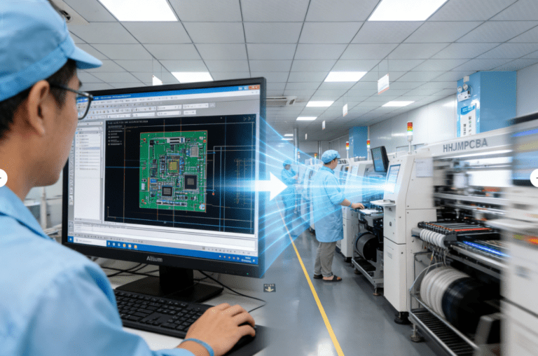
Stop worrying about how to design a pcb that might fail during manufacturing. At HCJMPCBA, we provide professional circuit board layout and pcb fab services that prioritize yield, reliability, and long-term PCBA services performance.
- Free DFM (Design for Manufacturing) Review
- Rapid 24-Hour Engineering Response
- One-Stop “Design-to-Delivery” Solution
Why Hardware Leaders Choose HCJMPCBA for PCB Board Design?
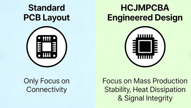
To succeed in today’s market, design printed circuit boards requires more than just connecting dots. It requires a deep understanding of the pcb design process. While competitors focus on simple connectivity, HCJMPCBA PCBA services integrate manufacturing intelligence into the earliest stages of designing pcb.
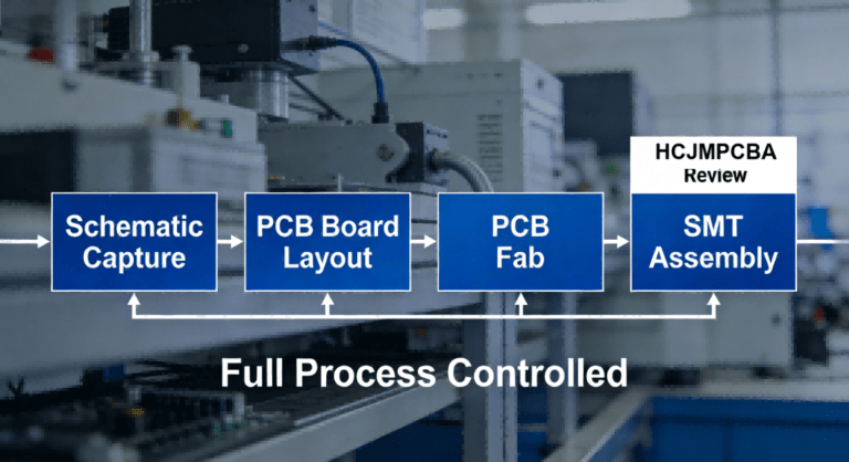
PCB Design and Layout Workflow
- Schematic Analysis and Requirement Definition
- Stack-up Planning and Material Selection
- Component Placement Optimization
- High-Speed Routing and Impedance Control
- DFM and DFA Validation
- Gerber Generation and Final Verification
Comprehensive PCB Design Flow: From Schematic to Fabrication
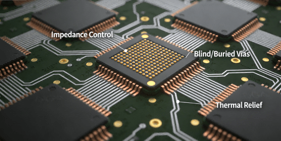
Technical Capabilities: Solving Complex Design Challenges
Beyond Files: The HCJMPCBA Mass Production Guarantee
Most agencies stop after handing over the Gerber files. We don’t. Our HCJMPCBA PCBA services include a long-term commitment to your product’s reliability.
- Standardized Method Numbers: Every project is assigned a unique Method Number + Revision. This ensures that even 5 years from now, your production batch will be identical to the first.
- Data-Driven Quality: We provide Raw Data for every critical step, from impedance coupons to reflow profiles.
- Global Traceability: Our Traceability (lot/batch/serial) system means every component on every board is documented.
| Design Factor | Basic Layout | Industrial-Grade Layout (HCJMPCBA) |
|---|---|---|
| Stack-up Planning | Generic | Application-specific impedance modeling |
| DFM Validation | Post-design | Integrated during layout |
| Signal Integrity | Basic routing | Controlled impedance + return path optimization |
| Traceability | None | Lot/Batch/Serial linked design files |
| Evidence Type | What It Proves |
|---|---|
| DFM Report | Manufacturability validation |
| Impedance Report | Signal integrity compliance |
| Gerber Files | Design output accuracy |
| Traceability Logs | Full production tracking |
Frequently Asked Questions: Expert Insights for PCB Procurement
1. How can I optimize my PCB design pcb costs for high-volume mass production?
The most effective way to reduce hdi pcb price and overall manufacturing costs is through early-stage DFM (Design for Manufacturing). At HCJMPCBA, we audit your pcb board layout to minimize layer counts, optimize panel utilization, and select cost-effective materials like high-Tg FR4 or BT resins without compromising signal integrity. Designing a pcb with manufacturing limits in mind can reduce waste by up to 15%.
2. What critical steps are involved in the HCJMPCBA pcb design flow?
Our pcb design process is an integrated engineering cycle:
- Schematic Capture & BOM Audit: Verifying component lifecycles.
- PCB Board Design & Routing: Optimizing for SI/PI.
- DFM/DFT Review: Applying a 100-point industrial checklist.
- Method Assignment: Every project receives a unique Method Number + Revision to lock in production parameters, ensuring that pcb board fabrication is perfectly repeatable.
3. How does HCJMPCBA handle high-density interconnect (HDI) and IC board design?
We specialize in complex high density interconnect pcb architectures, including elic pcb (Every Layer Interconnect) and stacked microvias. Our engineers utilize advanced pcb layout design software to manage fine-pitch BGA fan-outs and impedance control, ensuring your ic board design meets the rigorous requirements of 5G, medical, and aerospace applications.
4. What is the benefit of a “Factory-Integrated” pcb design service?
Unlike standalone design houses, HCJMPCBA PCBA services are directly connected to our SMT lines. This eliminates the “blame game” between designer and manufacturer. By designing pcb files in the same ecosystem where they are built, we can guarantee that test conditions and sample plans are optimized for the specific machinery used in our Guangzhou facility, leading to a much higher first-pass yield.
5. Can you perform reverse engineering or circuit board layout from a physical sample?
Yes. For legacy systems where documentation is lost, we offer professional design printed circuit services from physical samples. We recreate the circuit board layout, generate new Schematics/Gerbers, and perform a full pcb design basics audit to ensure the new version is compatible with modern pcb fab standards and components.
6. How do you ensure batch-to-batch consistency for long-term projects?
Reliability in mass production comes from Traceability (lot/batch/serial). Every board we produce is linked to a specific Method Number, which records the exact Raw Data from lamination, drilling, and reflow. This means whether you order 1,000 units today or 10,000 units next year, the test conditions and manufacturing “DNA” remain identical.
7. What file formats and software do you support for pcb board design?
Our engineering team is proficient in all industry-standard pcb layout design tools, including Altium Designer, Cadence Allegro, Mentor Graphics PADS, and KiCad. Whether you are providing a rough sketch for pcb design for beginners or a complex multi-layer high density interconnect file, we can adapt to your internal pcb design process.
8. How do I get a professional DFM report for my pcb board fabrication?
Simply submit your Gerber files or native design files through our portal. As part of our HCJMPCBA PCBA services, we provide a complimentary, comprehensive DFM audit within 24 hours. We don’t just tell you there is an error; we provide pcb examples and technical solutions on how to design a circuit board that is optimized for our high-speed SMT lines.
9.What is included in PCB design services?
It includes schematic capture, layout design, DFM validation, and production-ready file generation.
10.How do you ensure PCB design reliability?
Through controlled Method Numbers, test conditions, and full traceability systems.
11.Can PCB design affect production yield?
Yes. Poor design leads to defects, while optimized layouts ensure stable mass production.
Get Started: From Prototype to Mass Production

Ready to scale your hardware? Whether you need a simple design printed circuit board or a multi-layer high density interconnect masterpiece, HCJMPCBA is your technical anchor.
- Free DFM Check: Submit your files for a professional yield audit.
- Volume Discounts: We specialize in transitioning startups from pcb design basics to high-volume market leaders.
| Verification Item | Purpose | HCJMPCBA Evidence |
|---|---|---|
| DFM Report | Check manufacturability | Detailed engineering feedback |
| Impedance Simulation | Ensure signal integrity | Controlled trace modeling |
| Gerber Validation | Prevent production errors | CAM review logs |
Final Call to Action (CTA)
For more information about PCBA services, please contact Guangzhou Huachuang Precision Technology(HCJMPCBA). Our engineering team will provide a tailored quote and DFM report within 24 hours.
Update triggers: standard revision changes / recurring questions / production checklist updates.


