BGA Assembly
HCJMPCBA’s Precision Solutions for High-Reliability Ball Grid Array Manufacturing & Rework
1. Introduction to BGA Assembly
Ball Grid Array (BGA) is a revolutionary packaging technology that replaces traditional perimeter leads (e.g., QFP, SOP) with an array of solder balls underneath the component, enabling unprecedented component density and thermal performance in modern electronics .
What is BGA?
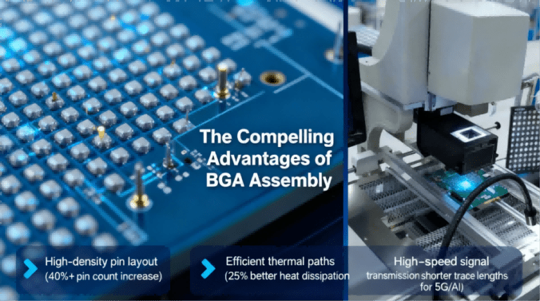
A BGA component features a grid of solder balls (typically 0.3–1.0mm diameter) that connect the chip to the PCB. This design:
- Increases pin count by 40%+ compared to QFP packages .
- Improves heat dissipation by 25% via direct thermal paths through solder balls .
- Reduces signal loss with shorter trace lengths, critical for high-speed applications like 5G and AI.
BGA vs. Traditional Packages: A Performance Comparison
| Attribute | BGA | QFP (Quad Flat Package) | SOP (Small Outline Package) |
|---|---|---|---|
| Pin Count | 100–2,000+ | 44–208 | 8–44 |
| Trace Length | ≤500μm | 1–2mm | 1–3mm |
| Heat Dissipation | 10–20W (with thermal vias) | 5–10W | 2–5W |
| Typical Applications | 5G modems, FPGAs, medical implants | Microcontrollers, basic DSPs | Logic gates, simple amplifiers |
The BGA manufacturing process involves four critical stages, each demanding precision and control:
Stage 1: CAD Design & Gerber Preparation
- Key Parameters:
- Solder ball pitch: 0.3mm (min), 0.4–1.0mm (standard) with ±0.02mm tolerance .
- Pad diameter: 60–80% of ball diameter (e.g., 0.4mm ball → 0.24–0.32mm pad).
- Thermal via placement: ≤2mm spacing, 0.3mm diameter (filled with solder mask or copper).
- Design Tools: Altium Designer, Cadence Allegro, ensuring DFM (Design for Manufacturability) compliance.
Stage 2: Solder Ball Preparation
- Materials:
- SAC305 (Sn96.5Ag3.0Cu0.5): Melting point 217°C, ideal for high-reliability applications .
- Pb-containing alloys (Sn63Pb37): Lower melting point (183°C) for legacy systems.
- Ball Formation: Precision stamping or reflowing, with diameter tolerance ±0.05mm.
Stage 3: Ball Placement (Balling)
- Methods:
- Laser Balling: 99.8% yield, suitable for fine-pitch (≤0.4mm) BGAs .
- Screen Printing: Cost-effective for ≥0.5mm pitch, with ±0.1mm placement accuracy.
- Inspection: Automated optical inspection (AOI) verifies ball count, size, and coplanarity (≤0.05mm variation).
Stage 4: Electrical & Mechanical Testing
- X-Ray Inspection: Verifies internal connections, solder voids (≤20% acceptable per IPC-A-610) .
- Thermal Cycling: -40°C to +125°C, 500 cycles to ensure solder joint reliability.
3. BGA Assembly Technology: Step-by-Step Precision
BGA assembly in PCBA manufacturing involves four core processes, each optimized for accuracy:
Step 1: SMT Placement
- Equipment: Yamaha YSM20R pick-and-place machines with ±0.01mm accuracy .
- Process:
- PCB alignment via fiducials (±0.02mm accuracy).
- BGA component pickup with vacuum nozzles (customized for ball grid pattern).
- Placement onto PCB with real-time vision alignment.
Step 2: Reflow Soldering
- Temperature Profile:
- Preheat: 150–200°C (60–90 seconds).
- Peak: 235–245°C (10–20 seconds).
- Cooling: ≤3°C/second to prevent thermal shock .
- Atmosphere: Nitrogen (99.9% purity) to minimize oxidation.
Step 3: Inspection & Testing
- AOI (Automated Optical Inspection): Detects open circuits, shorts, and insufficient solder with 100% coverage .
- X-Ray Inspection: Verifies solder joint integrity, voids, and alignment.
- Electrical Testing: Flying probe or bed-of-nails for 100% continuity check.
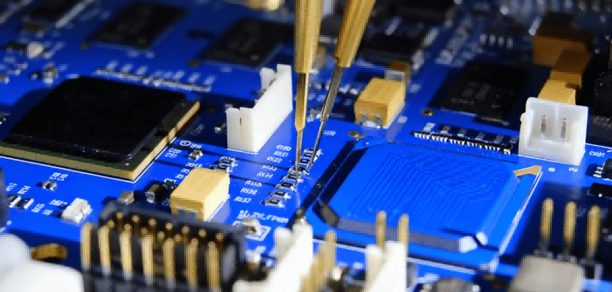
Step 4: Rework & Repair
- Equipment: IR (Infrared) rework stations (e.g., ERSA HR600) with precise temperature control.
- Process:
- Heat component to 250–260°C (above solder melting point).
- Remove defective component and clean pads.
- Apply new solder paste and reattach component.
- Yield: 95%+ for successful rework .
4. Optimal Solder Joints in BGA Assembly: Defects & Solutions
Achieving high-quality BGA solder joints requires strict control over materials, process, and environment. Below is a breakdown of common defects and remedies:
| Defect | Cause | Solution | IPC-A-610 Class 3 Compliance |
|---|---|---|---|
| Cold Joints | Insufficient peak temperature, slow heating rate | Adjust reflow profile (increase peak temp by 5–10°C) | Fail (no cold joints allowed) |
| Bridging | Excess solder paste, misaligned stencil | Reduce solder paste thickness (0.1–0.15mm), calibrate stencil | Fail (no bridging allowed) |
| Voids | Trapped flux, improper reflow | Use low-void solder paste, optimize reflow cooling rate | Pass (≤20% void area per joint) |
| Non-Wetting | Contaminated pads, oxidized solder balls | Clean pads with isopropyl alcohol, use nitrogen reflow | Fail (full wetting required) |
BGA technology powers innovation across industries, with tailored solutions for unique requirements:
Consumer Electronics
- 5G Smartphones: 0.3mm pitch BGA for SoCs (e.g., Qualcomm Snapdragon) enables 30% smaller form factors while supporting 10Gbps data rates .
- Laptops: GPU BGAs with thermal vias (0.3mm diameter, 1.5mm spacing) dissipate 15W+ heat, enabling thinner designs.
Medical Devices
- Pacemakers: Biocompatible BGAs (ENIG finish, PI substrate) operate in 1cm³ spaces, meeting ISO 13485 standards for biocompatibility and reliability .
- Portable Ultrasound: High-density BGAs in transducers enable 128+ channels in pocket-sized devices.
Automotive Electronics
- ADAS Radar Modules: BGAs with 0.4mm pitch withstand -40°C to +150°C temperature swings, ensuring reliable performance in harsh environments .
- EV BMS (Battery Management Systems): BGAs monitor 100+ cells with ±1mV voltage accuracy, critical for battery safety.
Industrial & Aerospace
- Factory Automation: FPGA BGAs in PLCs (Programmable Logic Controllers) support 10,000+ I/O points for complex manufacturing processes.
- Satellites: Radiation-hardened BGAs operate in -150°C to +120°C orbit conditions, with 10+ year lifespans.
6. BGA Design Considerations: HCJMPCBA’s Expert Guidelines
Designing for BGA assembly requires attention to layout, thermal management, and manufacturability. Use the HCJMPCBA BGA Design Checklist to avoid common pitfalls:
| Design Aspect | Best Practice | Common Mistake |
|---|---|---|
| Solder Ball Pitch | ≥0.4mm (0.3mm requires advanced processes) | 0.3mm pitch without process validation |
| Power/Ground Planes | Overlap with BGA area by ≥80% | Insufficient plane coverage (causes signal noise) |
| Thermal Vias | Diameter ≥0.3mm, spacing ≤2mm, filled with copper | Unfilled vias (cause heat buildup) |
| Trace Routing | Impedance-controlled (50Ω/100Ω), length-matched within 5mil | Uncontrolled impedance (causes signal reflection) |
| Component Placement | Keep BGAs ≥500μm from board edges | BGAs too close to edges (causes warpage) |
7. HCJMPCBA’s BGA Assembly Capabilities
As a leading BGA assembly manufacturer, HCJMPCBA delivers industry-leading precision and reliability:
| Capability | Technical Specification | Business Benefit |
|---|---|---|
| Fine-Pitch BGA | 0.3mm pitch, 99.2% assembly yield | Enables miniaturization for 5G and IoT devices |
| Quality Certifications | ISO 13485 (medical), IATF 16949 (automotive) | Qualifies for regulated industries (medical, automotive) |
| Turnaround Time | 24-hour BGA prototype, 5–7 days for production | Accelerates product development cycles |
| Inspection Technology | 3D AOI + X-Ray (Yxlon Cheetah) | Ensures 100% defect detection |
| Material Expertise | SAC305, Sn63Pb37, lead-free/high-temperature alloys | Tailors solutions to thermal and environmental needs |
| Rework Capability | 95%+ rework success rate | Reduces scrap costs for high-value components |
8. FAQs About BGA Assembly
1. What is the difference between BGA and uBGA?
uBGA (Ultra BGA) is a subset of BGA with ultra-fine pitches (≤0.3mm) and smaller form factors, typically used in mobile processors (e.g., Apple A17 Pro) . Standard BGAs have pitches ≥0.4mm.
2. How to choose BGA ball material for high-temperature applications?
For operating temperatures >125°C, use high-temperature alloys like Sn10Sb (melting point 232°C) or Pb-containing Sn90Pb10 (melting point 183°C for rework flexibility) .
3. BGA rework vs. BGA assembly: Cost comparison?
BGA rework costs 2–3x more than original assembly due to labor intensity and risk of PCB damage . For high-value components (e.g., FPGAs), rework is cost-effective; for low-cost ICs, replacement is better.
4. What is BGA assembly in PCBA manufacturing?
BGA assembly is the process of mounting Ball Grid Array components onto PCBs, involving solder paste application, precise placement, reflow soldering, and rigorous inspection . It enables high-density, high-performance electronics.
5. BGA assembly quality control guidelines for medical PCB?
Follow IPC-A-610 Class 3 and ISO 13485 standards:
- 100% X-Ray inspection for solder joints.
- Thermal cycling testing (-40°C to +85°C, 1,000 cycles).
- Biocompatibility testing for solder and substrate materials .
6. What is “turnkey BGA assembly” for prototypes?
Turnkey BGA assembly includes full service: component sourcing, PCB fabrication, BGA mounting, testing, and delivery—ideal for rapid prototyping (e.g., 24-hour turnaround for PCBA prototypes) .
7. How to calculate BGA assembly cost?
Cost factors include:
- Component pitch: Finer pitches (0.3mm) cost 20–30% more.
- Volume: Low-volume (1–100 units) costs $50–$200 per BGA; high-volume (10,000+ units) costs $5–$20 per BGA.
- Inspection: X-Ray adds 10–15% to total cost .
HCJMPCBA combines precision engineering with industry-specific expertise to deliver BGA solutions that meet the most demanding requirements:
- Accuracy: 0.3mm pitch BGA assembly with ±0.01mm placement accuracy.
- Speed: 24-hour prototyping to keep your project on schedule.
- Compliance: ISO 13485 and IATF 16949 certifications for medical and automotive applications.
- Reliability: 99.2% first-pass yield backed by rigorous testing.


