HDI PCB
HCJMPCBA’s Advanced High Density Interconnect Solutions for Next-Gen Electronics
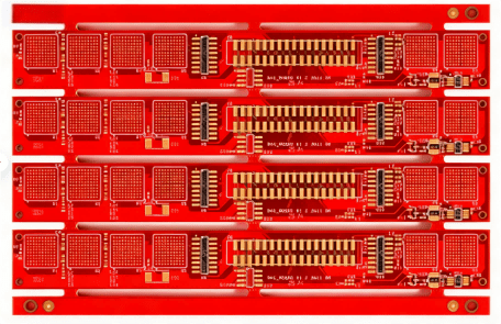
1. Introduction to HDI PCB
High Density Interconnect (HDI) PCB represents the pinnacle of printed circuit board technology, enabling unprecedented component density, miniaturization, and performance in electronic devices. Unlike traditional PCBs, HDI PCBs leverage microvias (blind, buried, or through vias with diameters as small as 50μm), fine-pitch traces (≤3mil), and stacked/sequential lamination to pack more functionality into smaller spaces .
Technical Evolution of HDI PCB
The journey of HDI PCB began in the late 1990s, driven by the mobile phone industry’s demand for thinner, more compact devices. Early iterations focused on single-layer microvia structures, but advancements in laser drilling, plating, and lamination now support any-layer HDI designs—where vias connect any layer, not just adjacent ones . This evolution has made high density interconnect PCBs indispensable for 5G smartphones, medical implants, and aerospace electronics.
How HDI PCB Differs from Traditional PCB
| Aspect | HDI PCB | Traditional PCB |
|---|---|---|
| Via Type | Microvias (50–150μm diameter); blind/buried/stacked vias | Through-holes (≥150μm diameter); limited layer connectivity |
| Trace Width/Spacing | 2–3mil / 2–3mil (≥50μm) | 5–8mil / 5–8mil (≥125μm) |
| Component Density | Supports 01005 (0.4×0.2mm) components; BGA pitches ≤0.3mm | Limited to 0603 (1.6×0.8mm) components; BGA pitches ≥0.5mm |
| Layer Count | 2–50 layers (any-layer connectivity) | 2–32 layers (layer-to-layer connectivity only) |
| Typical Applications | 5G phones, pacemakers, drone controllers | Computers, industrial controls, basic consumer electronics |
2. Types of HDI PCB
HDI PCBs are classified by their layer structure, microvia configuration, and manufacturing complexity. Below is a detailed comparison of the most common types:
| HDI Type | Layer Structure | Microvia Configuration | Process Complexity | Typical Applications |
|---|---|---|---|---|
| 1+N+1 HDI | 1 microvia layer + N core layers + 1 microvia layer | Single-layer microvias (no stacking) | Low | Basic smartphones, IoT sensors, entry-level wearables |
| 2+N+2 HDI | 2 microvia layers + N core layers + 2 microvia layers | Stacked microvias (2 layers deep) | Medium | Mid-range smartphones, medical monitors, automotive infotainment |
| Any-Layer HDI | Multiple microvia layers with connections to any layer | Stacked, staggered, and buried microvias | High | 5G flagship phones, pacemakers, aerospace avionics |
| Mixed-Signal HDI | Combination of digital, analog, and RF layers | Controlled-impedance microvias; RF-optimized traces | Very High | 5G base stations, radar systems, test & measurement equipment |
3. HDI PCB Manufacturing Process
The fabrication of HDI PCBs involves specialized processes to achieve microvia precision and layer connectivity. Below is a step-by-step breakdown:
Step 1: Laser Drilling
- Equipment: UV laser drills (e.g., LPKF MicroLine) with pulse widths as short as 10ns.
- Process:
- Drills microvias (50–150μm diameter) through dielectric layers.
- Depth control: ±5μm for blind vias; ±10μm for buried vias.
- Yield: 99.5% for defect-free microvias .
Step 2: Desmear & Microvia Plating
- Desmear: Removes resin smear from laser-drilled holes using plasma or chemical processes.
- Pulse Plating: Deposits copper into microvias with:
- Current density: 2–4 A/dm².
- Thickness: 20–30μm (ensures reliable conductivity).
- Uniformity: ≥90% across the panel.
Step 3: Build-Up Lamination
- Material: Prepreg (FR4 or high-Tg) and copper foil (1/2–1oz).
- Process:
- Stack layers with precise alignment (±10μm).
- Cure under heat (170–200°C) and pressure (25–40 bar).
- Repeat for sequential build-up (up to 20 layers).
Step 4: Fine-Line Imaging & Etching
- Imaging: Uses LDI (Laser Direct Imaging) for trace widths/spacings as low as 2mil.
- Etching: Chemical etching (acid or alkaline) with:
- Etch factor: ≥3.0 (vertical etch with minimal undercut).
- Uniformity: ±10% across the panel.
Step 5: Surface Finish & Testing
- Surface Finish: ENIG (Electroless Nickel Immersion Gold), OSP, or immersion silver.
- Testing:
- Electrical: Flying probe (100% continuity).
- Structural: X-ray (verifies microvia integrity).
- Reliability: Thermal cycling (-40°C to +125°C, 500 cycles).
4. HDI PCB Industry Standards & Compliance
Adherence to industry standards is critical for HDI PCB reliability, especially in medical and automotive sectors. Below are key standards and their impact:
| Standard | Scope | Key Requirements | Business Impact |
|---|---|---|---|
| IPC-2226 | Design standard for HDI PCBs | – Microvia aspect ratio (1:1 max) – Trace width/spacing (≥2mil) – Stacked via alignment (±10μm) |
Reduces design errors by 35%; ensures interoperability |
| IPC-6012D | Performance standard for rigid PCBs | – Copper thickness (≥18μm) – Solder mask coverage (≥95%) – Thermal shock resistance (288°C, 10s) |
Lowers field failure rate by 40% in automotive/medical devices |
| ISO 13485 | Medical device manufacturing | – Traceability (batch-to-material) – Cleanroom manufacturing (Class 10,000) – Biocompatibility testing |
Enables entry into regulated medical markets; boosts trust |
| IATF 16949 | Automotive manufacturing | – APQP (Advanced Product Quality Planning) – PPAP (Production Part Approval Process) – Process capability (Cpk ≥1.33) |
Qualifies suppliers for Tier 1 automotive projects; ensures consistency |
5. Applications of HDI PCB
HDI PCBs enable innovation across industries by solving space, performance, and reliability challenges:
Consumer Electronics
- 5G Smartphones: 12-layer 3 阶 HDI PCBs in devices like the iPhone 15 Pro enable 30% volume reduction while integrating 5G modems, AI chips, and cameras .
- Foldable Devices: Samsung Galaxy Z Fold5 uses any-layer HDI to create flexible hinges with 100,000+ bend cycles.
Medical Devices
- Pacemakers: Biocompatible HDI PCBs (ENIG finish, PI substrate) fit into 1cm³ spaces, delivering life-saving pulses for 10+ years .
- Portable Ultrasound: HDI PCBs in devices like the Butterfly iQ+ enable pocket-sized scanners with hospital-grade imaging.
Automotive
- ADAS Systems: Radar modules in Tesla’s Autopilot use HDI PCBs with 50Ω controlled impedance to detect objects 200m away.
- Electric Vehicles: Battery management systems (BMS) rely on HDI PCBs to monitor 100+ cells with ±1mV voltage accuracy.
Aerospace & Defense
- Satellite Components: HDI PCBs in SpaceX’s Starlink satellites withstand -150°C to +120°C temperature swings in orbit.
- Military Radios: Ruggedized HDI PCBs in handheld radios operate in dust, moisture, and vibration (MIL-STD-810G certified).
6. HDI PCB Design Considerations
Designing HDI PCBs requires careful planning to balance density, performance, and manufacturability. Use the HCJMPCBA HDI PCB Design Checklist below to avoid common pitfalls:
| Design Aspect | Best Practices | Common Mistakes |
|---|---|---|
| Stackup Planning | – Use symmetric stackups (e.g., 2+4+2) to minimize warpage – Allocate 1–2 layers for power/ground planes – Choose high-Tg (170°C+) material for thermal stability |
– Asymmetric layer counts (causes warpage) – Thin cores (≤0.2mm) in high-stress areas |
| Microvia Design | – Keep microvia aspect ratio ≤1:1 – Stagger stacked vias (offset ≥50μm) – Use filled vias for high-current paths |
– Stacked vias without offset (causes shorting) – Unfilled vias in signal-critical areas |
| Trace Routing | – Maintain trace width ≥2mil (50μm) – Use gradual curves instead of right angles – Implement differential pairs with 100Ω impedance |
– Narrow traces (≤1.5mil) in high-current paths – 90° bends in RF traces (causes signal reflection) |
| Component Placement | – Keep BGAs ≥500μm from board edges – Place heat-generating components (e.g., CPUs) near vias – Use solder mask dams between adjacent pads |
– BGAs too close to edges (causes delamination) – No thermal vias under power ICs (overheating) |
| Impedance Control | – Single-ended: 50Ω ±10% – Differential: 100Ω ±10% – Use impedance calculators (e.g., Polar SI9000) |
– Ignoring impedance in high-speed signals – Inconsistent trace width in controlled paths |
7. HCJMPCBA’s HDI PCB Capabilities
As a leading HDI PCB manufacturer, HCJMPCBA combines cutting-edge technology with rigorous quality control to deliver industry-leading solutions:
| Capability | Technical Specification | Business Benefit |
|---|---|---|
| Layer Count | 2–32 layers (any-layer HDI available) | Supports complex designs for 5G and AI applications |
| Microvia Size | 50–150μm diameter; aspect ratio 1:1 max | Enables ultra-dense packaging (01005 components, 0.3mm BGAs) |
| Trace Width/Spacing | 2mil / 2mil (50μm / 50μm) min | Supports high-speed signals (up to 112Gbps PAM4) |
| Turnaround Time | 24-hour prototype; 5–7 days for production | Accelerates product development cycles |
| Quality Certifications | ISO 9001, ISO 13485, IATF 16949 | Qualifies for medical, automotive, and aerospace projects |
| Yield Rate | 99.2% first-pass yield | Reduces rework costs and delivery delays |
| Material Options | FR4, high-Tg FR4, PI, Rogers (for RF) | Tailors solutions to thermal, electrical, and mechanical needs |
8. FAQs About HDI PCB
1. What is the cost difference between HDI PCB and traditional PCB?
HDI PCBs cost 20–50% more than traditional PCBs due to specialized processes (laser drilling, sequential lamination). However, they reduce overall product cost by enabling smaller enclosures, fewer components, and lower assembly fees.
2. How to ensure 5G signal integrity in HDI PCB?
- Use controlled-impedance traces (50Ω for single-ended, 100Ω for differential).
- Implement ground planes adjacent to RF traces.
- Use low-loss materials (e.g., Rogers 4350B) for RF layers.
- Minimize via stubs and use backdrilling for long vias .
3. What design tools are best for HDI PCB?
Altium Designer, Cadence Allegro, and Mentor Graphics PADS support advanced HDI features like microvia planning, stackup management, and impedance simulation.
4. Can HDI PCBs be used for high-power applications?
Yes. Use:
- Thick copper (2–6oz) for power planes.
- Filled vias for current-carrying paths.
- Thermal vias (≥1mm diameter) under power ICs.
5. What is the minimum order quantity (MOQ) for HDI PCB?
HCJMPCBA has no strict MOQ—we support 1-piece prototypes and 100,000+ unit production runs.
6. How to choose between 1+N+1 and any-layer HDI?
- 1+N+1: Best for cost-sensitive, low-complexity designs (e.g., basic smartphones).
- Any-Layer: Ideal for high-density, high-performance applications (e.g., 5G base stations, medical implants).
7. What is the typical lifespan of an HDI PCB?
With proper design and manufacturing, HDI PCBs last 10–20 years in consumer electronics and 20+ years in industrial/medical devices.
As a trusted HDI PCB manufacturer and supplier, HCJMPCBA delivers:
- Precision: 2mil trace/spacing and 50μm microvias for extreme density.
- Speed: 24-hour prototypes to keep your project on schedule.
- Quality: ISO 13485 and IATF 16949 certifications for regulated industries.
- Expertise: A decade of experience in high density interconnect PCB design and manufacturing.


