Unveiling the Power of Intelligent Feeder Racks in Modern Electronics Manufacturing at Guangzhou Huachuang Precision Technology Co., Ltd.
Guangzhou Huachuang Precision Technology Co., Ltd. has introduced intelligent feeder racks to provid
As electronics grow in complexity—with higher speeds, denser routing, stricter EMI / signal integrity constraints—many designs now require more than 4 or 6 layers. 8 layer pcb stackup offers a powerful middle ground: more routing flexibility than simpler boards, with manageable cost and manufacturing complexity compared to ultra high-layer count designs. In this article, we explore what is an 8 layer pcb stackup, how it’s typically structured, and how to design one effectively from material choice to signal / power layout, impedance control, thermal considerations, and best practices.
By following this guide, OEM engineers, procurement decision-makers, and PCBA integrators will be better equipped to specify, review, or partner on high-performance multilayer PCBs.
–Routing capacity: More internal layers relieve congestion, especially when you have many signals or dense BGA packages.
–Improved signal integrity: With multiple ground / power planes adjacent to signal layers, you get better return path control and lower crosstalk.
–Better power distribution / decoupling: Dedicated planes for power and ground reduce voltage drop and noise.
–EMI / EMC control: Multiple shielding planes between signals help suppress electromagnetic interference.
–Thermal handling: Internal copper planes assist in heat spreading and dissipation.
–Mechanical stability: A symmetric, balanced 8 layer board can reduce warpage in lamination.
Hence designs requiring high speed (e.g. DDR, SerDes), dense interconnect, or stringent EMI demands often adopt 8-layer stackups.
–High-performance motherboards or control boards
–FPGA / SoC boards with multiple high-speed interfaces
–Telecom / networking equipment
–Industrial control & instrumentation with mixed analog / digital / power sections
–Medical electronics, communications modules
In these use cases, multi layer pcb becomes essential.
There is no single standard, but a commonly used stackup layout is:
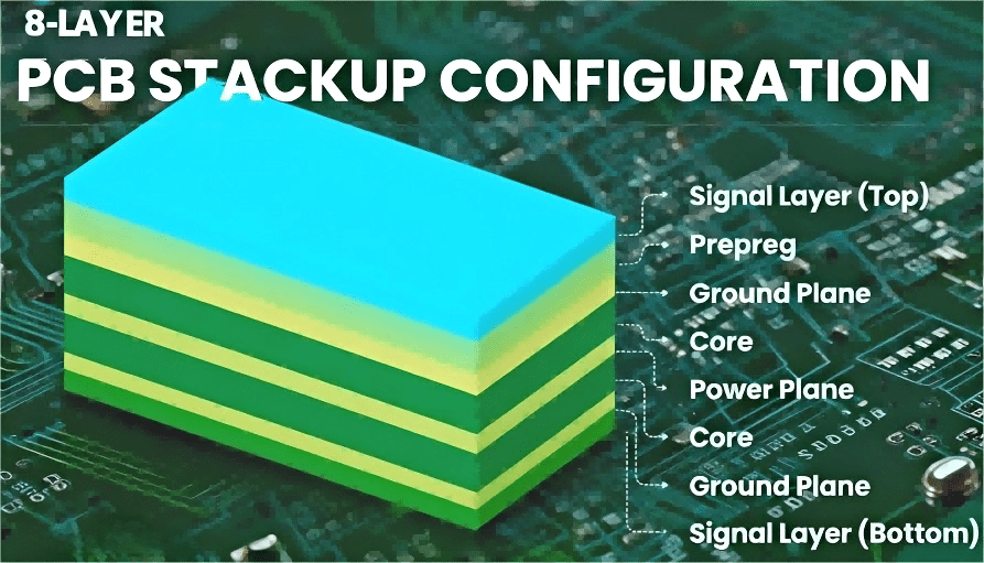
Hcjmpcba 8 Layer Pcb Stackup Configuration
Or more elaborated:
–Layer 1: Top signal
–Layer 2: Ground plane
–Layer 3: Signal
–Layer 4: Ground / plane
–Layer 5: Power plane
–Layer 6: Signal
–Layer 7: Ground plane
–Layer 8: Bottom signal
One forum user posted a similar structure:
“TOP, GND, SIG1, GND, PWR, SIG2, GND, BOTTOM” Reddit
In that arrangement, each high-speed signal layer is adjacent to a reference plane (ground), which improves return path control and lowers interference. This principle—signal layers abutting ground or power planes—is widely accepted in stackup design. SierraConnect
Alternate variations may insert extra signal layers or use split planes depending on routing demands, but the core remains: signal ↔ reference plane adjacency and balance / symmetry to avoid warpage.
Layer stackup is not just about copper; the dielectric materials (prepreg, cores) and their dielectric constant affect impedance, spacing, and performance. You must specify appropriate prepreg or core materials (often FR-4 or high TG variants) and thickness to meet impedance targets.
Typical 8 layer pcb thicknesses range from around 1.6 mm (0.063 in) to 2.0 mm or more, depending on the stackup, copper weights, and dielectric layers used. Some designs push thinner, but yield and manufacturability challenges increase.
Copper weights (outer / inner) also influence current carrying capacity, thermal dissipation, and power plane integrity. For example, you might use 1 oz outer + 1 oz inner or heavier copper on power planes. The thickness directly impacts impedance margins and mechanical robustness.
To ensure board integrity and minimize warpage, the stackup should be symmetrical when possible: the layers above the center should mirror those below. This balance matters during lamination, thermal cycling, and mechanical stress.
Poor symmetry or ground/power plane splits can lead to bending, warping, or delamination.
For high-speed signals, every trace ideally rides adjacent to a continuous reference plane (often ground). This ensures that the current return path is short and tightly coupled, reducing loop area and coupling to other signals.
In an 8 layer stackup, placing signal layers next to ground planes is a widely accepted best practice, as highlighted in engineering discussions. SierraConnect
When you design high-speed nets (USB, DDR, PCIe, SerDes), you must do impedance control. The combination of trace width, dielectric spacing, and copper thickness determines characteristic impedance (e.g. 50 Ω, 100 Ω differential).
To minimize crosstalk, adjacent signal layers should route orthogonally or be shielded by solid planes. Keep spacing and guard bands where needed.
Signal layers are often paired or grouped such that you route differential pairs or matched length nets in middle signal layers. The inner layers, when sandwiched between planes, form striplines; outer signal layers form microstrips.
Proper layer adjacency and plane pairing reduce signal distortion and help maintain signal integrity.
In an 8-layer design, you can allocate dedicated planes for ground and power. A good practice is to keep power planes solid and contiguous, avoiding splits unless absolutely necessary. Splits in planes can create return path discontinuities, harming high-speed performance.
Via stitching connects power/ground planes across layers and helps reduce impedance. Decoupling capacitors should be placed close to power pins and connected via shortest paths to reference planes.
Ensure good via fanout, and consider thermal / current handling in plane design.
Plane islands or significant splits within power or ground layers break current paths and can cause signal integrity issues. Each signal or power net must have a continuous reference.
An internal plane can act as a heat spreader; thermal vias connect hot components to internal copper for better heat distribution. The more internal copper you have, the more you can dissipate heat.
–Through vias: go through all layers—simple but consume routing space
–Blind / buried vias: connect to specific inner layers to save surface routing area
–Via in pad: places via inside the component pad, useful for high density but complicates manufacturing
–Keep via aspect ratios (board thickness : hole diameter) within manufacturer capabilities
More layers and vias increase manufacturing complexity. Check your PCB vendor’s capability for lamination, via tolerances, registration, and yield. Stackup tolerances, misregistration, and thermal expansion must be controlled.
A symmetrical layer structure helps reduce warpage but also balances electromagnetic properties. Good symmetry in multi layer pcb stackup helps reduce coupling and emission.
Use ground stitching around edges, guard traces between noisy nets, and shield zones beneath sensitive areas. Avoid slotting in planes and avoid placing high-speed traces that cross splits in planes.
Where analog, digital, RF domains exist, careful segmentation is needed, but segments must maintain return continuity. Avoid unnecessary isolation that breaks reference paths.
Here is a recommended process:
1.Requirements gathering (signal count, speed, power rails, mechanical constraints)
2.Select initial stackup (choose layer arrangement, dielectric materials, copper weights)
3.Simulate impedance / return paths using tools or field solvers
4.Place components / partition zones to reduce cross-domain interference
5.Route critical nets first, route high-speed with reference adjacency
6.Plan vias, stitching, decoupling early
7.DRC + SI / EMI review and adjustment
8.Finalize and hand off to manufacturing, verifying stackup in fabrication docs
Throughout, maintain collaboration with your PCB / PCBA manufacturer to verify lamination constraints, minimum spacing, via capabilities, and stackup viability.
Q: Can I treat 8-layer PCB like 6 layers with two extra layers?
A: Not exactly. The extra layers must be properly placed for signal/ground adjacency, and decisions about which pairs to use affect noise, EMI, and return paths.
Q: 1.2 mm vs 1.6 mm stack — which to choose?
A: Thinner boards (1.2 mm) save space but challenge impedance margin and via geometry. 1.6 mm thickness is safer for most standard 8-layer designs.
Q: What is the “8th layer” typically used for?
A: In many designs, it’s a signal or routing layer, often lower-speed or breakout nets, protected by adjacent ground planes.
Q: Does increasing layer count dramatically increase cost?
A: Yes — more layers require more materials, precise lamination, registration control, and possibly yield losses.
Q: How to choose stackup when working with HCJMPCBA services?
A: Provide your signal, power, and mechanical requirements. Our engineering team will propose suitable 8 layer pcb stackup with material & cost tradeoffs.
An 8 layer pcb stackup offers a balanced, powerful solution for complex, high-speed, dense designs. It gives routing freedom, improved signal integrity, EMI control, and better thermal performance—provided you plan carefully.
Key principles:
–Place signal layers adjacent to reference planes
–Use symmetric, balanced designs
–Choose proper materials, copper weights, and board thickness
–Plan via strategy and thermal paths
–Incorporate EMI mitigation and verify with simulation
When designing or ordering PCBs for demanding projects, knowing and controlling the 8 layer pcb stackup is essential. If you want professional stackup design, advanced multilayer capability, or tailored PCBA manufacturing support, please contact Guangzhou Huachuang Precision Technology (HCJMPCBA).
Guangzhou Huachuang Precision Technology Co., Ltd. has introduced intelligent feeder racks to provid
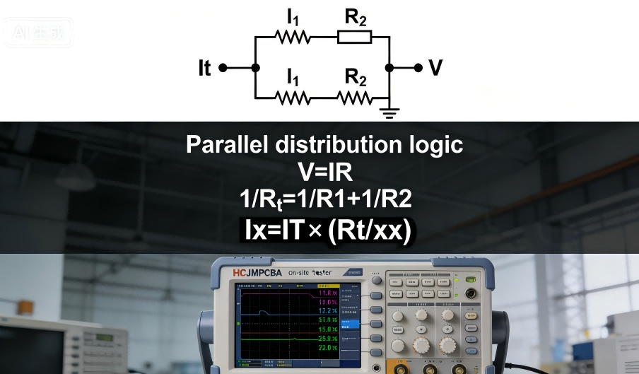
This guide breaks down the current divider and voltage divider formulas, explaining their core diffe
Guangzhou Huachuang Precision Technology Co., Ltd. offers diverse electronics manufacturing solution


