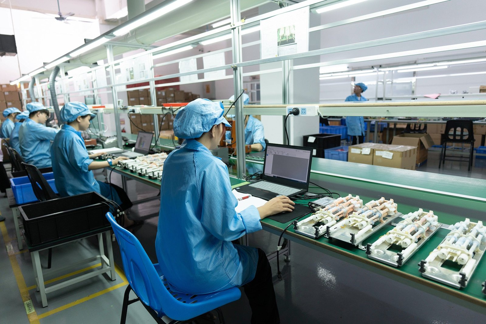
Understanding the Foundations of PCB Assembly and Soldering
1.1 What Is PCB Assembly?
PCB assembly involves mounting electronic components—resistors, capacitors, ICs—onto a printed circuit board, then creating solder joints that connect each pin or lead to its copper pad. Unlike mere board fabrication, assembly integrates component placement, soldering, and testing into a cohesive workflow.
1.2 Why Proper Soldering Matters
Improper soldering leads to common failure modes:
-
Cold Solder Joints: Dull, grainy appearance; high electrical resistance.
-
Bridging: Unwanted solder blobs shorting adjacent pins.
-
Tombstoning: One end of a chip lifts off the pad due to uneven wetting.
Reliable solder joints maintain signal integrity, withstand thermal cycling, and ensure long‑term durability—critical for applications from medical devices to aerospace controls.
2: Preparing for Soldering a Circuit Board
2.1 Workspace and Tool Setup
A well‑organized bench reduces errors and improves consistency:
-
ESD‑Safe Environment: Anti‑static mat, wrist strap, and ionizer protect sensitive chips.
-
Fume Extraction: Local exhaust prevents inhalation of flux vapors.
-
Lighting & Magnification: A 5–10× loupe or microscope reveals joint details.
Essential Tools:
-
Soldering iron (30–60 W) with temperature control
-
Fine conical or chisel tip (0.5–1.0 mm)
-
Lead‑free solder wire (SnAgCu, 0.5 mm diameter)
-
No‑clean or water‑soluble flux paste
-
Tweezers, solder wick, and desoldering pump
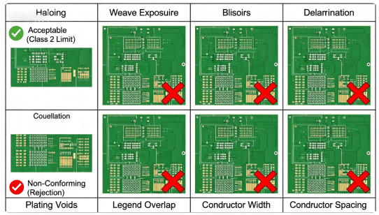
2.2 PCB and Component Inspection
Before soldering, ensure:
-
Clean Copper Pads: Wipe with isopropanol to remove oxidation and residues.
-
Component Verification: Match each device’s polarity, orientation, and footprint.
-
Pad Integrity: Check for lifted pads or incomplete etching using a magnifier.
3: 5-Step PCB Board Soldering Process
Achieving repeatable, high‑quality joints requires a systematic approach:
-
Tin the Iron & Apply Flux
-
Heat the iron to 350 °C (for lead‑free solder).
-
Wipe the tip on a wet sponge, then coat it with fresh rosin flux or solder wire.
-
Pre‑Tin Pads and Leads
-
Place and Align Components
-
Make the Solder Joint
-
Touch both pad and lead with the iron tip simultaneously.
-
Feed solder wire into the joint—not onto the iron—until a smooth fillet forms.
-
Withdraw solder first, then the iron, to avoid cold joints.
-
Inspect and Clean
-
Inspect under 10× magnification: joints should be shiny and conical.
-
Remove residual flux with isopropanol and a soft brush, especially for high‑voltage or medical boards.
Pro Tip: For fine‑pitch ICs and pcb board soldering on motherboards, consider hot‑air reflow or stencil printing to ensure uniform solder volume.
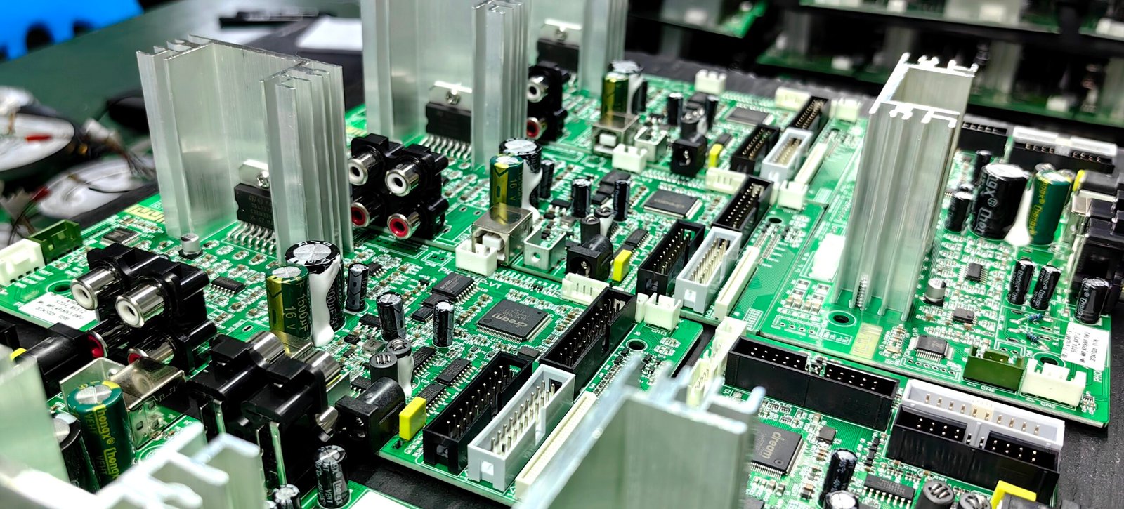
4: Advanced Techniques: Soldering on a Motherboard & Repair Strategies
4.1 How to Solder on a Motherboard
Working on multi‑layer, high‑density boards (like motherboards) demands:
-
Hot‑Air Rework Stations: Use a defined airflow and calibrated nozzle to reflow BGA, QFP, and QFN packages.
-
Pre‑Heating Platens: Gentle bottom‑side heating (80–100 °C) reduces thermal shock.
-
Solder Paste Stencils: Apply consistent solder volume for complex components.
4.2 PCB Circuit Board Repair Best Practices
Repairing damaged traces or joints involves:
-
Desoldering Faulty Parts: Use solder wick and braid with moderate heat to remove old solder cleanly.
-
Trace Repair: Bridge broken copper tracks with 30 AWG insulated wire or conductive epoxy.
-
Pad Replacement: Rescue lifted pads by gluing a replacement pad from a donor board and soldering it in place.
These methods restore functionality without compromising long‑term reliability.
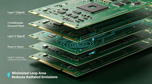
5: Material Selection & Thermal Profiling for High‑Reliability Joints
5.1 Choosing the Right Solder Alloy
-
Sn96.5Ag3.0Cu0.5 (SAC305): Widely used lead‑free alloy balancing strength and melting point.
-
Sn63Pb37: Preferred for prototyping due to lower melting temperature (183 °C) and shiny joints—though phased out in medical and aerospace.
5.2 Thermal Profiling Essentials
-
Ramp‑Soak‑Spike Curve: Gradually increase temperature to soak zone (150–180 °C), then spike to peak (235–245 °C) for 30–60 s.
-
Thermocouple Mapping: Place probes on critical components—large BGAs and fine‑pitch QFNs—to verify uniform heating.
Proper profiling minimizes voids, tombstoning, and thermal stress on delicate components.
6: Case Study: Music Instrument Control PCB Soldering
An advanced guitar‑effects pedal PCB required ultra-low noise and compact form factor:
This project showcased how meticulous soldering a circuit board elevates both mechanical reliability and signal fidelity in high‑end audio electronics.
7: Choosing the Right Partner for High‑End PCB Assembly
Selecting a pcb assembly supplier goes beyond soldering skills; look for:
A partner with these capabilities ensures your circuit board soldering and assembly projects meet the highest performance and reliability standards.
Conclusion & CTA
Whether you’re learning how to solder a circuit board or seeking a turnkey pcb assembly partner, mastering both fundamentals and advanced techniques is key. From precise thermal profiling to expert pcb circuit board repair, excellence in soldering underpins every successful electronic product.
For more information about PCBA services, please contact Guangzhou Huachuang Precision Technology.