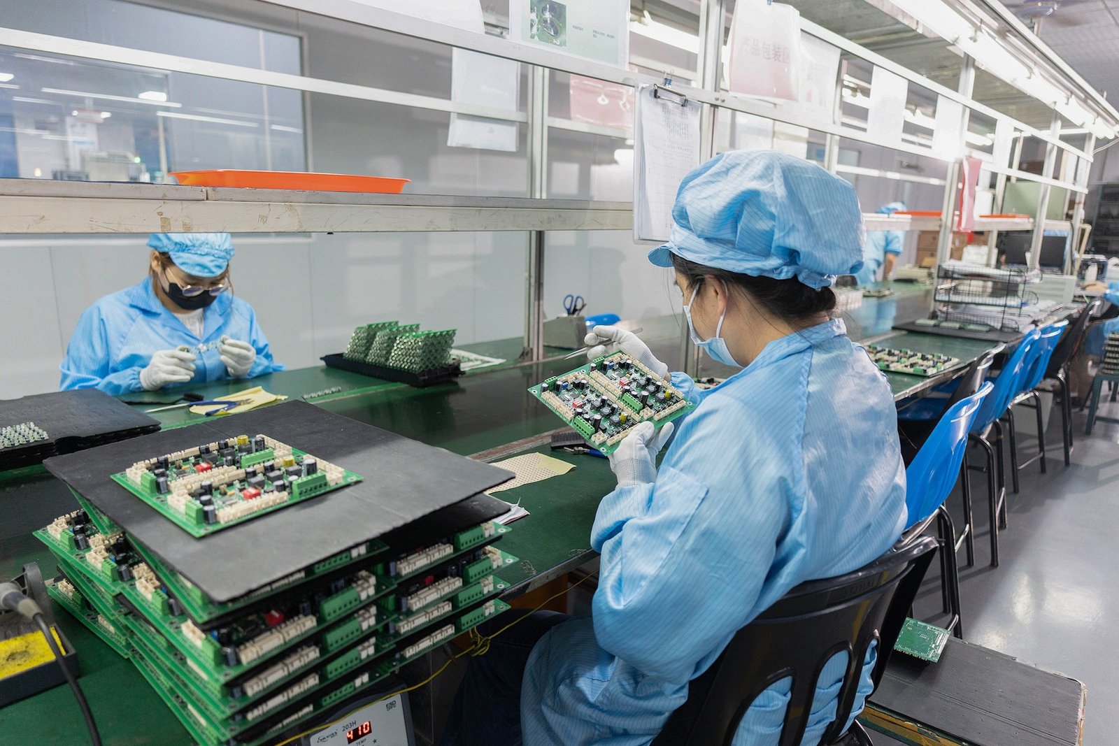
High-Precision Electronics Assembly Workshop: Serving Medical, AI, Energy & Industrial Markets
The article provides an in-depth look at the advanced equipment,rigorous processes,skilled workforce
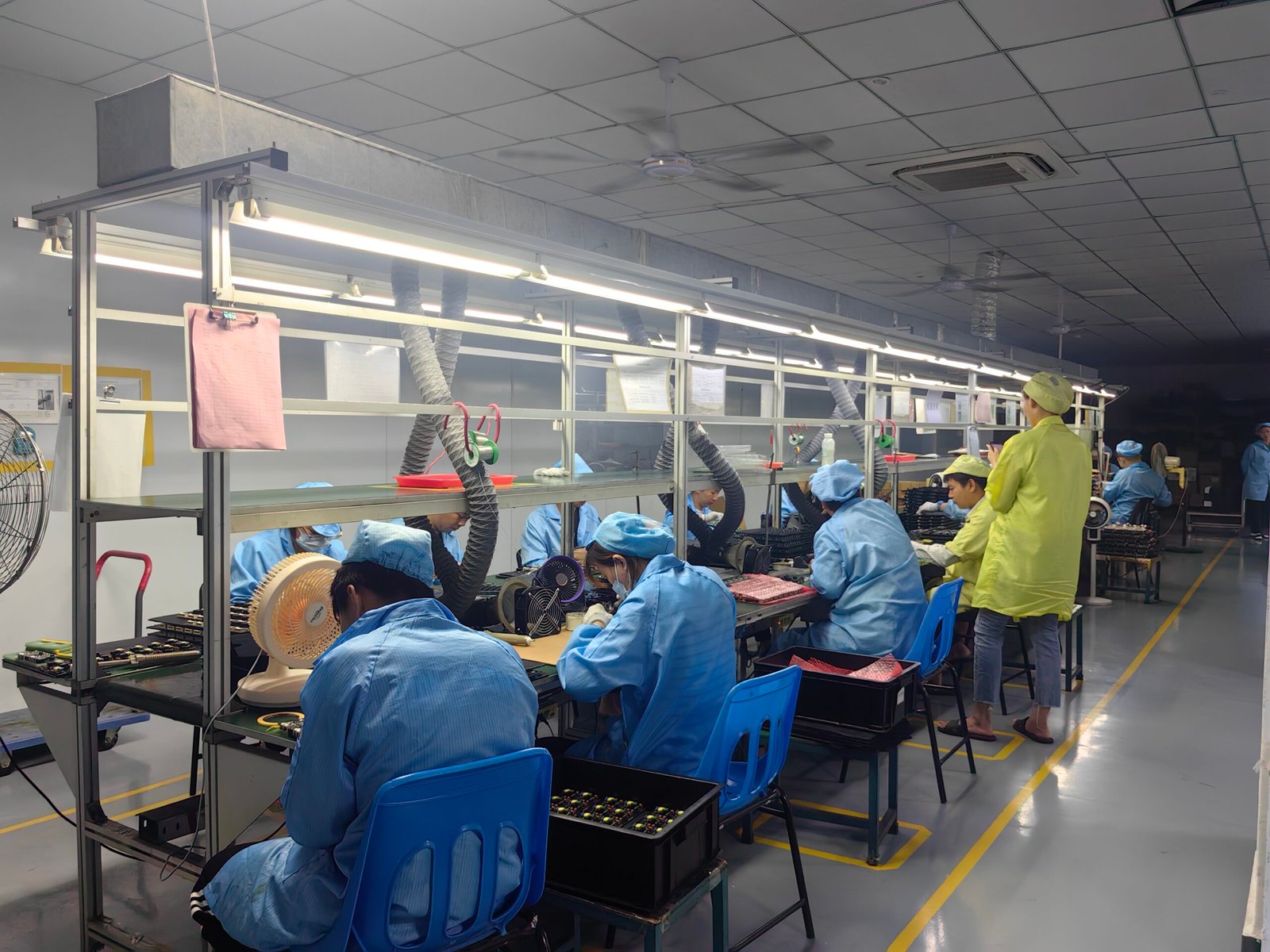
In modern SMT PCB assembly, the backbone is the automated pick-and-place machine, which accurately positions SMDs onto solder-printed boards at rates exceeding 30,000 components per hour. Equally crucial is solder paste printing via stencil printers, ensuring paste volume and alignment meet tight tolerances to avoid tombstoning or solder bridges. Following placement, reflow soldering ovens apply precise temperature profiles—preheat, soak, reflow and cooling—to melt paste and form reliable joints without damaging parts . Finally, inspection stations like SPI (Solder Paste Inspection), AOI (Automated Optical Inspection) and X-ray ensure any defects are caught early, reducing rework and scrap rates.
Surface-mount technology (SMT) revolutionized electronics by mounting components directly on the PCB surface, enabling miniaturization and higher circuit density . Compared to through-hole, SMT supports faster line speeds and lower labor costs, making it ideal for high-volume production of consumer, medical and industrial PCBs Key SMT processes include: solder paste printing, pick-and-place, reflow soldering, cleaning (if needed), and final inspection/test. Advanced variants—like jet-printing for ultrafine pitch and no-clean pastes—further boost yield for cutting-edge microelectronics.
Main equipment for microelectronics surface mount technology
Stencil Printer – applies solder paste via stainless-steel stencil for consistent deposit.
Pick-and-Place Machine – high-speed placement with vision systems for sub-0.05 mm accuracy.
Reflow Oven – convection or vapor-phase ovens with multi-zone heating for precise thermal profiles.
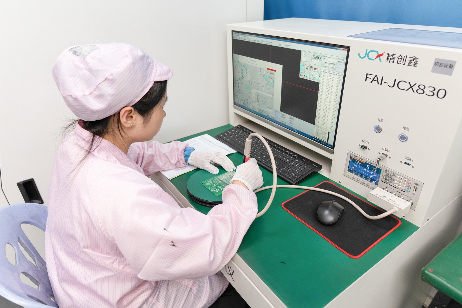
Solder Paste Inspection (SPI) – 3D SPI systems measure paste volume and shape to catch print defects.
Automated Optical Inspection (AOI) – inspects component presence, polarity and solder joint quality.
X-Ray Inspection – checks hidden joints (BGAs, QFPs) for voids and misalignments.
In-Circuit Test (ICT) – electrical test to verify assembly functionality and catch shorts/open circuits.
Fine-Pitch Placement for pitches below 0.5 mm, relying on high-resolution cameras and ultra-precise feeders.
Jet-Printing Solder Paste, which allows stencil-free printing for 0201 components and complex shapes.
No-Clean and Low-Void Pastes, designed to minimize post-reflow residue and void formation under BGAs.
Adaptive Soldering Profiles, where real-time thermocouples adjust conveyor speed or zone temperatures on the fly.
Inline 3D X-Ray and SPI Fusion, combining volumetric paste data with 3D X-ray joint inspection for end-to-end defect capture.
Hcjmpcba Pcb3
SMT PCB assembly is a high-speed, high-precision dance between paste, placement, heat and inspection. By leveraging advanced printers, pick-and-place systems, reflow ovens and in-line inspection technologies, HCJM delivers microelectronics solutions that balance throughput, quality and cost—making us your go-to partner for complex SMT PCB needs in the US market.
The article provides an in-depth look at the advanced equipment,rigorous processes,skilled workforce
This article focuses on "what is pcb assembly", systematically introduces the classification, compon
Guangzhou Huachuang Precision Technology Co., Ltd. (HCJMPCBA) specializes in ISO 13485-certified Bl