Unveiling the Power of Intelligent Feeder Racks in Modern Electronics Manufacturing at Guangzhou Huachuang Precision Technology Co., Ltd.
Guangzhou Huachuang Precision Technology Co., Ltd. has introduced intelligent feeder racks to provid
I often get asked, “What is PCB assembly?” Beyond soldering parts onto a board, understanding the circuit diagram is the first step toward a successful build. In this post, I’ll walk you through how circuit diagrams are classified, what they’re made of, and how you—yes, you—can read them with confidence.
Circuit diagrams come in a few flavors, each serving different purposes:
Schematic Diagrams show the electrical relationships with symbols and lines—think of them as the blueprint for connections.
Wiring Diagrams map out the physical layout of wires and connectors, helping you route cables on a real PCB.
Block Diagrams break the system into functional blocks (power, control, I/O) without getting bogged down in detail—great for high-level design reviews.
Pictorial Diagrams give you a more literal view, showing component shapes and orientations—handy when you’re first laying out parts.
Each type answers a specific question: “How are things wired?” vs. “What does each block do?” vs. “Where does this connector go?” I recommend starting with schematics, then referring to wiring or pictorial views as you move into layout.
Symbols for components: resistors, capacitors, ICs, connectors—they must follow standardized shapes so anyone can recognize them.
Connections (nets): straight or curved lines that link symbols. Pay attention to labels like “GND,” “VCC,” or net names—these tell you where signals and power go.
Annotations: values (e.g., “10 kΩ”), reference designators (“R1,” “U2”), and notes on voltage or test points. These details turn a blank schematic into a buildable plan.
When I lay out or review a design, I check that every symbol has a clear reference designator, no nets are left floating, and critical nets (like power rails) have appropriate labels. If you spot missing annotations, flag them before moving to layout!
Here’s my step-by-step approach when I first see a new schematic:
Identify Power Rails: Locate VCC, GND and any additional supplies. This gives you a reference frame.
Find Key Blocks: Spot power regulation, microcontroller or main IC sections, and I/O interfaces. Treat each block as its own mini-circuit.
Trace Signal Flow: Follow nets from inputs (sensors, connectors) through processing blocks to outputs (LEDs, motors). Ask yourself: “What happens to this signal?”
Check Component Values: Verify resistor and capacitor values make sense for the expected frequency or voltage. Out-of-range values often signal errors.
Look for Notes & Test Points: Make sure you know where to measure voltages or inject signals for debugging.
You can do this on paper or with your EDA tool’s highlighting feature. By the end, you should be able to explain each block’s function and how they all tie together—crucial before you start “what is pcb assembly” in the real world.

Understanding how to read circuit diagrams is the foundation for successful PCB assembly. By classifying diagrams, knowing their core components, and following a clear step-by-step approach, you’ll be ready to move from design to production with confidence. Next time someone asks, “What is PCB assembly?”, you can answer: it starts on paper with a well-understood schematic, and that’s exactly where HCJM’s expertise shines.
Guangzhou Huachuang Precision Technology Co., Ltd. has introduced intelligent feeder racks to provid

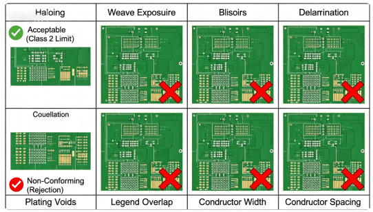
Learn why 100% AOI inspection is critical in high-mix low-volume (HMLV) PCB assembly. This guide exp
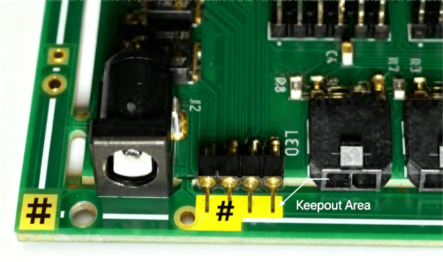
A keepout on a PCB is a software-enforced exclusion zone that prevents copper, vias, or components i