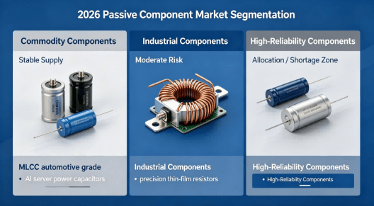
2026 Global Resistor and Capacitor Market Reality: Supply Pressure, Price Volatility, and Engineering-Level Risk Control in PCB & PCBA Manufacturing
Direct Answer The global resistor and capacitor market in 2026 is no longer a stable commodity envir
Circuit board design is the backbone of modern electronics, enabling the functionality of devices ranging from smartphones to medical equipment. Understanding the intricacies of designing a printed circuit board (PCB) is essential for engineers, procurement professionals, and decision-makers in the electronics industry.
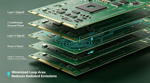
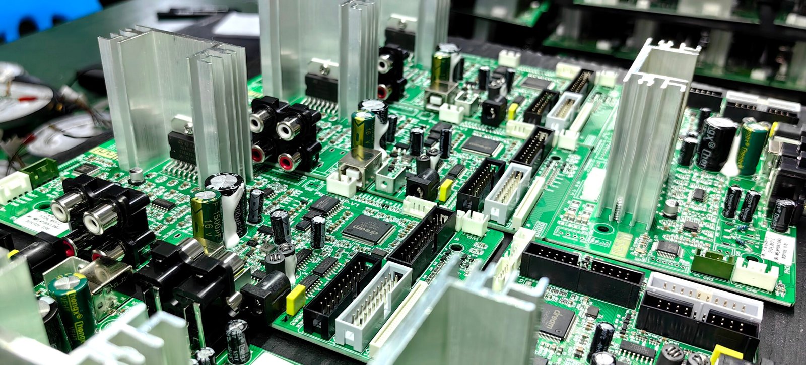
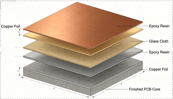
A circuit board, or PCB, is a flat, rigid structure that electrically connects and mechanically supports electronic components. It consists of conductive pathways, or traces, etched from copper sheets laminated onto a non-conductive substrate. PCBs can be single-sided, double-sided, or multi-layered, depending on the complexity and requirements of the electronic device.
The design process begins with a thorough understanding of the project’s specifications, including electrical parameters, mechanical constraints, and environmental considerations. This phase ensures that the final design meets all functional and regulatory requirements.
Engineers create a schematic diagram that represents the electrical connections between components. This blueprint serves as the foundation for the PCB layout and guides the placement of components and routing of traces.
Choosing the right components is crucial for the performance and reliability of the PCB. Factors such as voltage ratings, current capacities, and thermal characteristics must be considered to ensure compatibility and durability.
In this phase, the physical arrangement of components on the board is determined. Designers place components strategically to optimize space, minimize signal interference, and facilitate efficient routing of electrical connections.
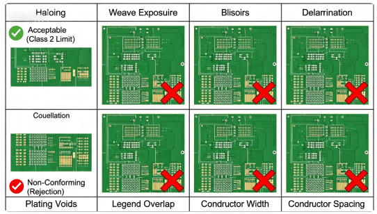
A design rule check is performed to verify that the layout adheres to manufacturing constraints, such as trace width, spacing, and hole sizes. This step helps prevent errors that could lead to functional failures or manufacturing delays.
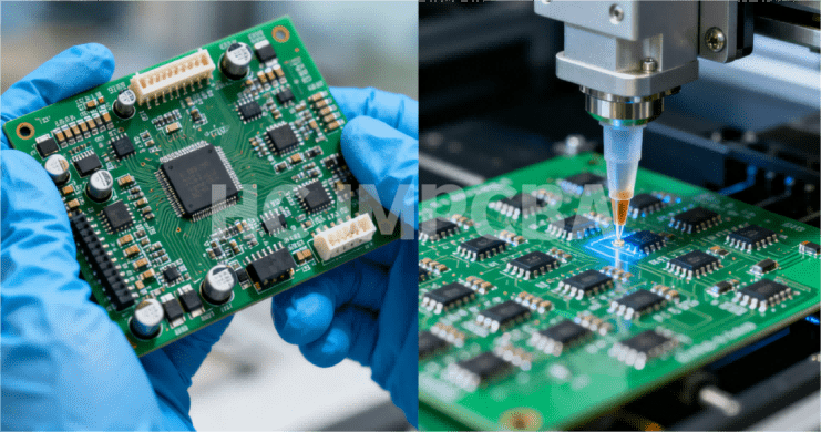
A prototype PCB is fabricated and assembled to validate the design. Testing involves checking electrical performance, signal integrity, and thermal behavior to ensure the PCB operates as intended.
Once the prototype passes testing, the final design files are prepared for mass production. This includes generating Gerber files, Bill of Materials (BOM), and assembly drawings, which are used by manufacturers to produce and assemble the PCBs.
Signal Integrity: Ensuring clear and reliable signal transmission by minimizing noise and interference.
Thermal Management: Designing for effective heat dissipation to prevent component overheating and failure.
Electromagnetic Compatibility (EMC): Implementing design strategies to minimize electromagnetic interference with other devices.
Design for Manufacturability (DFM): Adhering to manufacturing constraints and standards to facilitate efficient production and assembly.
Selecting a dependable PCB supplier is critical for ensuring the quality and timeliness of your projects. Consider the following factors:
Experience and Expertise: Choose suppliers with a proven track record in PCB manufacturing and a deep understanding of industry standards.
Quality Assurance: Ensure the supplier has robust quality control processes in place, including testing and inspection procedures.
Manufacturing Capabilities: Verify that the supplier can handle your specific design requirements, such as multi-layer boards or high-frequency applications.
Customer Support: Assess the supplier’s responsiveness and willingness to collaborate throughout the design and manufacturing process.
Artificial Intelligence (AI) Integration: AI is being utilized to automate design processes, detect errors, and optimize layouts, reducing development time and costs.
Flexible and Wearable Electronics: Advancements in materials and manufacturing techniques are enabling the development of flexible and stretchable PCBs for wearable devices.
High-Frequency and High-Speed Designs: The demand for high-speed data transmission is driving innovations in PCB design to handle higher frequencies and reduce signal loss.
Q1: What is the difference between a PCB and a PCBA?
A PCB (Printed Circuit Board) is the bare board with no components, while a PCBA (Printed Circuit Board Assembly) includes the PCB with all components soldered onto it.
Q2: How can I ensure my PCB design is manufacturable?
Collaborate closely with your PCB supplier during the design phase to adhere to design for manufacturability (DFM) guidelines.
Q3: What software tools are commonly used in PCB design?
Popular tools include Altium Designer, KiCad, Eagle, and OrCAD.
Understanding the nuances of circuit board design is essential for creating reliable and efficient electronic products. By following a structured design process and collaborating with experienced suppliers, you can ensure the success of your PCB projects.→HCJMPCBA RFQ
For more information on PCB design and manufacturing services, please contact HCJMPCBA.→HCJMPCBA Facebook
Direct Answer The global resistor and capacitor market in 2026 is no longer a stable commodity envir
Guangzhou Huachuang Precision Technology Co., Ltd. excels in PCBA processing. It starts with order a
Learn how to select the right FR4 ANSI plate for PCB projects in this engineering guide. Understand