How to Design Coplanar Waveguide with Ground in Your PCB: Mastering kicad how to draw curved coplanar waveguide
Learn kicad how to draw curved coplanar waveguide with ground plane backing to achieve precise imped
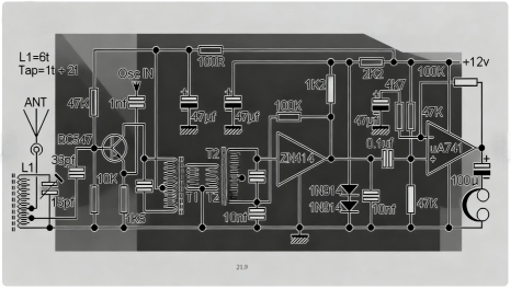
When someone refers to a wiring diagramt, they are typically talking about an electrical schematic—a symbolic representation of how electrical components are connected and interact across a system. According to standard references, a circuit diagram (synonym) “is a graphical representation of an electrical circuit” using standardized symbols rather than physical layout.
A wiring diagramt often emphasizes the physical wiring and connection paths of a system—showing how wires, terminals, connectors link components.
An electrical schematic focuses on the electrical relationships: how components functionally interconnect, not necessarily their physical placement.
A circuit diagram is a more general term: “wiring diagram, electrical diagram, elementary diagram, electronic schematic” are all referenced.
An electrical wiring diagram tends to describe detailed wiring instructions, often for installation or assembly rather than conceptual design.
For a PCB/PCBA engineer, the distinction matters: you often work from the electrical schematic (function) to the PCB layout (physical). Recognising the keyword wiring diagramt helps ensure that procurement and engineering discussions align precisely.
Understanding a well-structured schematic enables you to spot risks early: missing nets, symbol misinterpretation, layout-to-schematic mismatches. Next, we’ll dive into how to interpret the building blocks: symbols and connections.
Common Standards For Electronic Symbols
A high-quality schematic is the blueprint of a circuit—showing components, nets, power rails, ground, signal flow and functional blocks. As one tutorial puts it: “An electrical schematic is a graphical representation of an electrical circuit, using standardized symbols to depict components and their connections.”
In PCB/PCBA manufacturing and sourcing, the schematic serves multiple roles:
Design intent: how the circuit is supposed to behave
Documentation: specification for layout, assembly, test
Communication tool: bridging engineering, procurement, test, manufacturing
Reference for verification: checking that layout matches schematic and BOM
Wiring schematic diagram / wiring diagramt – emphasises wiring paths, connectors, terminals
Electrical schematic diagram – emphasises component function and net relationships
Circuit diagram / circuit drawing symbols – broad term, often used in education/troubleshooting
Electrical installation diagram – used in installations and systems rather than PCBs
Electrical schematic drawings / electrical drawing – documentation notation
Recognising the type of diagram helps you set appropriate review and verification criteria.
The standardized use of electrical symbols facilitates clarity and international collaboration. For instance, an “electronic symbol” is defined as “a pictogram used to represent various electrical and electronic devices or functions” in schematic diagrams.
If you misinterpret a symbol for a diode, transistor, or connector, you risk misrouting, sourcing wrong parts or mis-specifying the manufacturing process.
For a PCB/PCBA engineer, familiarizing yourself with the following is essential:
Power/ground symbols: battery, DC supply, earth, chassis
Passive components: resistors, capacitors, inductors
Active components: transistors (BJT/FET), diodes, ICs
Connectors & terminals: header pins, wire harness, plugs
Wiring/terminals: junctions, cross-points, net labels
As one source notes: “The symbols used in schematic diagrams are according to standards … such as IEC 60617, ANSI Y32.2‐1975, IEEE Std 91/91a.”
When reading an electrical connections diagram (or wiring schematic), attention should be paid to:
Net lines: these represent wires or traces linking components
Junctions (dots) vs crossings (no dot) – misinterpreting these can lead to unintended connections.
Reference designators (RefDes) – each symbol has a unique label (e.g., R3, C12) that corresponds to BOM and footprint. See “reference designator” standards.
Layout flow: traditionally, signal flow is depicted left-to-right, power (high to low) top-to-bottom.
By mastering how to follow connections and read symbols, PCB engineers improve layout validation and manufacturability.
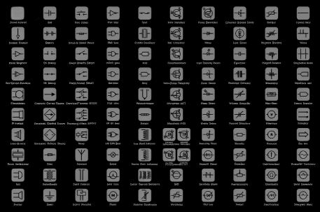
The Symbols Used In The Schematic Diagram Conform To The Standards
For a PCB/PCBA engineer, decoding a wiring schematic is a systematic exercise—one that should fit into your verification and design-review workflow. Below are five essential steps.
Begin by finding the main power supply symbol, its rails, ground references and connector entry points. Many failures trace back to flawed power domains or missing ground returns.
Check for multiple power domains (e.g., 3.3 V, 5 V, 1.2 V) and make sure their origin, regulation, decoupling and return paths are clear.
Next, break the schematic into logical functional blocks (input interface, signal processing, output stage, connectors, test points). Understanding these helps you follow signal flow in the next steps.
Experienced engineers recommend “seeing the different ‘blocks’ of the circuit” as an efficient way to interpret schematics.
Follow nets from left to right (where possible) and top to bottom.
Look for net labels and annotations, priority flags (reset, enable, etc.)
Recognize wire crossings and confirm whether they are connected or simply crossing (junction dot convention)
Confirm connectors: correct pin numbers, orientation, harnesses
Match RefDes and parts list: each symbol should correspond to BOM and layout footprint
Once nets are traced, interpret each symbol:
Does R5 form a pull-up, filter or load resistor?
Is C12 for decoupling, coupling or timing?
Are symbols annotated with values, tolerances, footprints?
Is the part number in BOM consistent with symbol?
Practice: one UI engineer observed that once you understand sticker symbols and local conventions, you can read schematics without referencing a textbook.
For PCBA manufacturing, after reading the schematic, the engineer should verify:
That the PCB layout matches the schematic nets (netlist check)
That connectors/pins correspond to board footprints and assembly drawings
That test points, manufacturing pads, ISP/I/O harnesses present in schematic correspond to board test strategy
That mechanical clearance, keepouts, and board outline are informed by schematic (especially wiring and harness regions)
Reading the wiring schematic diagram in this disciplined way ensures layout, assembly and procurement downstream are correctly aligned.
From the perspective of a PCB/PCBA engineer or procurement decision-maker, comprehending the wiring diagramt has tangible value in the manufacturing lifecycle.
Layout validation: Engineers produce PCB layout files based on schematic nets. Mis-read schematic = mis-routed board → late correction.
BOM sourcing & procurement: Symbols and part numbers in schematic inform procurement of correct components. Misinterpretation increases sourcing risk.
Assembly/test planning: Wiring diagrams define connector pinouts, harnesses and test points. Clear diagrams speed up assembly and test fixture design.
Design review and DFM: Engineers reviewing schematic can spot manufacturability or testability issues early (ex: inadequate test-pin access, ambiguous connector wiring).
Supplier communication: When your manufacturing partner asks for an “electrical schematic drawing” you must deliver a document they can interpret across layout, fabrication, test and procurement.
Mis-interpreting wire crossings and junctions can lead to unintended net connections. Use consistent dot/no-dot rules.
Ignoring variant symbols across regions (US/Europe). Always confirm symbol library standard (IEC vs ANSI).
Not tracking connector pin numbers/back-annotation on PCB. Ensure schematic shows both logical and physical pinouts.
Lack of annotation or legend (“electrical symbols chart”) leaving engineers or assemblers guessing part functionality.
Layout not matching schematic nets (“how to read a PCB board” issue). One article emphasises the importance of reading the board by first understanding the schematic.
Insist that any submitted design includes a clean “electrical schematic diagram” with legend, symbol chart and net list.
In your review checklist, include: signal-flow left-to-right, ground at bottom, power at top; net labels clear; no ambiguous crossings.
For procurement, validate parts referenced in schematic against BOM and footprint libraries—don’t treat schematic as decorative.
During DFM review, use schematic to trace critical nets (power, high-speed, test points) and ensure board layout supports them.
To help you operationalize schematic reading and validation, here’s a best-practice checklist tailored for engineering teams and procurement in PCB/PCBA environments:
Adhere to standards
Use symbol standard sets (IEC 60617, ANSI Y32.2 etc.) to ensure clarity.
Maintain a comprehensive “electrical symbols chart” in the documentation package.
Maintain signal flow logic
Design/annotate schematic such that major signal flow goes from left to right; power rails top to bottom.
Avoid clutter, keep grouping logical, functional blocks visually separated.
Label nets, connectors, reference designators clearly
Each component must have unique RefDes (e.g., R1, C2, U3).
Net labels must be consistent and meaningful (e.g., “VDD_3V3”, “GND”).
Connectors and harnesses must show physical pin numbers and logical function.
Ensure schematic-to-layout traceability
Provide net list, BOM, PCB footprint mapping.
Post-layout review should match schematic nets and connectors without exception.
Perform “reading electrical drawings” hand-off reviews with layout engineers and procurement.
Include assembly/test facilitation
Indicate test points, probe pads, harness interfaces.
Where applicable, include an “electrical wiring diagram” of the harnesses or external wiring.
Ensure manufacturing/assembly staff have access to “wiring schematic symbols” legend and connector diagrams.
Version control and revision management
Maintain schematic revision history and change log (“reading schematics” related to revision control).
Any layout change must be back-annotated to schematic and documentation updated accordingly.
Cross-discipline review and communication
Engage mechanical, EMI/thermal and test teams in schematic review early.
Use the schematic as the communication hub: layout, sourcing, test, DFM teams all refer to the same document.
Do not rely solely on board‐silkscreen or layout drawings for function clarification.
How To Design A Professional Looking Schematic Diagram
Q: What is the difference between a wiring diagramt and a circuit diagram?
A: A wiring diagramt emphasises physical wiring and connection paths (especially for installation/harness), whereas a circuit diagram (or electrical schematic) emphasises functional connections and component behavior. In PCB/PCBA workflows both matter—but the schematic (functional) is the primary source for layout.
Q: How to read a wiring schematic diagram if I’m in procurement rather than engineering?
A: Focus on three elements:
Do the symbol labels (RefDes) match your BOM?
Are connectors clearly shown with pin numbers and logical function?
Are nets labelled and mapped to layout footprints?
If these align, you have a sound foundation for sourcing and assembly.
Q: Are electrical schematic symbols universal across regions (US/Europe)?
A: Symbols are largely standardised (e.g., IEC 60617, ANSI Y32.2) but regional variations exist. Always confirm which standard the schematic uses and ensure your team’s symbol chart aligns.
Q: I have a schematic but not a PCB layout – how can I validate before manufacturing?
A: You can perform a “desk review”: follow signal flow, trace power and ground rails, check nets and connectors. Then compare to layout file when available. Use netlists, BOMs and verify footprint mapping to eliminate surprises.
Q: How do I read a printed circuit board from the schematic?
A: First read the schematic to understand functional blocks; then locate the corresponding layout on the PCB. Use traces, silkscreen labels, refdes and test pads to map schematic components to board physical parts. The process is described in articles on reading circuit boards.
A wiring diagramt (electrical schematic) is the core document for tracking electrical connections, components and functionality in PCB/PCBA design.
Reading and understanding schematics enables engineers and procurement teams to spot risks early, validate layout/sourcing/test readiness, and streamline manufacturing.
Mastery comes from knowing electrical symbols, connection conventions, net flow logic, and how to cross-check schematic to layout.
In a PCB/PCBA environment, using best practices—standard symbols, clear net labelling, connector pin mapping, version control and cross-discipline review—ensures smooth hand-off from design to manufacture.
For OEM engineers and procurement leads, making schematic reading part of the review workflow significantly reduces layout errors, sourcing mismatches, and test failures.
Learn kicad how to draw curved coplanar waveguide with ground plane backing to achieve precise imped

Learn how HCJMPCBA ensures zero-defect PCBA through ISO 13485 compliance, IPC Class 3 standards, 3D

Explore what pcb design services entail—from schematic creation to Gerber file outputs. This compr