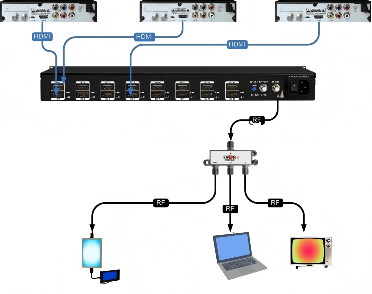
5 Powerful Insights into HDMI RF Modulators: How to Choose the Perfect Modulator for Coax Distribution
Curious about the HDMI RF Modulator? Learn how HDMI RF modulators convert HDMI signals into RF for c
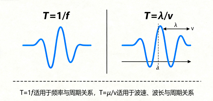
In electrical engineering, physics and high-speed PCB/PCBA design, understanding the period of a wave (often expressed as T) is fundamental. A wave’s period is the time it takes to complete one full oscillation or cycle. It is tightly linked to frequency (f): mathematically, T = 1 / f.
Unlike the wavelength (distance travelled per cycle), the period formula focuses on time. For engineers working on PCB traces, signal integrity or high-speed interfaces, knowing the period formula and its derivatives enables precise timing, matching trace lengths, avoiding reflections and ensuring clean signal transitions.
In practice, when you see a specification such as “clock signal at 2 GHz”, that immediately implies a period of T = 0.5 ns (since T = 1/2×10⁹). Then — through a second formula — you may determine how that corresponds to trace length (wavelength) and how fast the signal travels in your PCB substrate. Without this understanding, risk enters: inaccurate impedance matching, signal skew, EMI-issues and poor system performance.
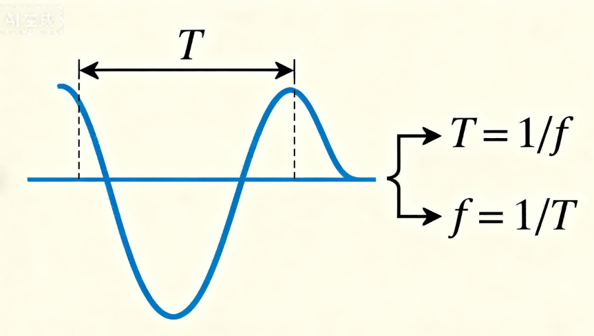
Frequency (f) Mathematically T = 1 F
The most direct expression of the period formula is:
T=1/f
Here T is the period in seconds (s), and f is the frequency in hertz (Hz).
Another commonly used variant, especially when you know wavelength (λ) and wave propagation speed (v), is:
T=λv\mathbf{T = \frac{\lambda}{v}}
This form is often called the wavelength period formula.
Understanding both forms enables you to flexibly compute the period from whatever variables you have.
T: period (s) – the time for one complete cycle.
f: frequency (Hz) – number of cycles per second.
λ (lambda): wavelength (m) – distance over which cycle repeats.
v: velocity (m/s) – propagation speed of wave.
Suppose a clock signal in your PCBA runs at 500 MHz. Then:
T=1500×106 Hz=2.0×10⁻⁹ s =2 nsT = \frac{1}{500 \times 10^6 \text{ Hz}} = 2.0 \times 10^{-9} \text{ s } = 2 \text{ ns}
Alternatively, if you know the signal’s wavelength in the PCB medium is 0.4 m and propagation speed is 2 ×10⁸ m/s (typical in FR-4 ~0.66 c), then:
T=0.4 m2×108 m/s=2.0×10−9 s =2 nsT = \frac{0.4 \text{ m}}{2 \times 10^8 \text{ m/s}} = 2.0 \times 10^{-9} \text{ s } = 2 \text{ ns}
This aligns perfectly with the first formula, confirming internal consistency.
T = 1f T = λv
When dealing with sinusoidal functions (common in signal integrity analyses), the period enters via the general form:
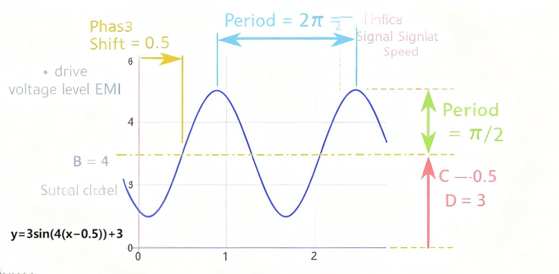
y=Asin(B(x+C))+Dy = A \sin\big(B(x + C)\big) + D
Here:
A is amplitude (height of wave) mathsisfun.com+1
B relates to the period: Period = 2π / B
C is phase shift, D is vertical shift.
For example, if the equation is y=3sin(4(x−0.5))+3y = 3 \sin(4(x − 0.5)) + 3, then the period = 2π/4 = π/2. Engineers analysing high-speed traces must account for amplitude (which drives voltage levels and EMI), phase shift (which may cause timing skew) and period (which influences how quickly the signal repeats).
This brings in long-tail keywords like “how to find amplitude”, “phase shift formula”, “amplitude period and phase shift”.
Period 2π B
High-speed PCBs and PCBA assemblies are essentially wave-transmission platforms. The electrical signal you send down a trace is not static; it exhibits a period, frequency, wavelength and amplitude much like any wave in physics.
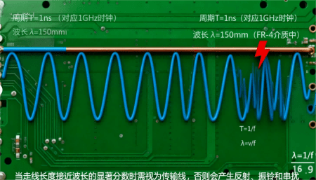
If a clock runs at 1 GHz, period T = 1 ns. The corresponding wavelength in PCB material (~150 mm for FR-4 at ~0.66 c) means that if your trace length approaches a significant fraction of that wavelength, you must treat the trace as a transmission line. Failure to do so can cause reflections, ringing, crosstalk and EMI. Keywords: “high speed pcb”, “pcb signal integrity”, “signal integrity in pcb design”.
Trace length matching: when multiple signals need synchronous arrival, the period sets constraints on length differences.
Material dielectric constant: affects propagation speed v and thus wavelength λ and period T = λ/v.
Via/trace design and carrying capacity: although current carrying capacity calculators (“pcb current”, “pcb via current calculator”, “carry capacity calculator”) handle DC or low-frequency, at high frequency the periodic behaviour dominates and must be integrated into design.
System-level timing: period sets the fundamental time unit for one cycle; designers must ensure rise/fall times, setup/hold margins, etc, align with that cycle.
A high-speed serial link at 2.5 Gbps implies bit period ~0.4 ns. If the PCB trace length corresponds to ¼ of the wavelength in the medium, significant reflections can occur. A manufacturer like HCJMPCBA must understand the wave period formula from T = 1 / f, the associated wavelength, and design the PCB stack-up, trace geometry and termination accordingly.
Here is a clear workflow for engineers or buyers:
Step 1: Identify frequency (f).
This is often given in the component datasheet (eg. clock 500 MHz) or can be measured.
Step 2: Use the primary period formula.
T=1fT = \frac{1}{f}
Example: f = 250 MHz → T = 1/250×10⁶ = 4 ns.
Step 3: If wavelength (λ) and velocity (v) are known, use the alternative formula.
T=λvT = \frac{\lambda}{v}
Example: λ = 0.3 m, v = 2×10⁸ m/s → T ≈ 1.5 ns.
Step 4: Apply to PCB trace length.
Compare trace length (L) to λ; if L > λ/10 or so, treat as transmission line and design with signal integrity in mind.
Keywords used: “how to find period”, “how to find the period of a function”, “equation for period”.
While calculators for current (e.g., via size calculators, carrying capacity calculators) focus on thermal and DC limits, for high-speed applications you must also inspect the wave period. If the periodic signal’s transition time approaches the period, then the via and trace geometry need extra attention (impedance discontinuities, reflections). Incorporate “pcb current”, “pcb via current calculator”, “carry capacity calculator” into the mechanical/thermal design, and period formula into the high-speed/time-domain design.
Schematic Diagram Of High Frequency Signal Propagation In Pcb
Designing based solely on frequency, ignoring period.
They may quote 1 GHz but don’t consider T = 1 ns and corresponding trace length/wavelength.
Choosing standard PCB materials without checking dielectric constant (Er).
A slower propagation speed (lower v) increases wavelength and period, causing mismatches in design expectations.
Neglecting phase shift and amplitude when computing period/wavelength.
Misuse of functions like y = A sin(B(x+C)) leads to wrong B value, wrong period. Keywords: “phase shift”, “amplitude period and phase shift”.
Assuming DC-design calculators suffice for high-frequency signals.
They may use “pcb current” or “via current calculator” tools, but overlook that period/wavelength may drive EMI and timing issues.
Real-world example: A PCBA supplier delivered boards where the trace length equalled ~⅓ λ at 2.4 GHz. Without termination or matching, repeated reflections occurred leading to signal dropouts. The fix required redesign of stack-up and trace geometry based on the period formula and corresponding wavelength.
Request a specification sheet that includes signal period/frequency, trace/via geometry, impedance control and stack-up dielectric constant.
Ask if the manufacturer has processes to control high-speed signals:
Controlled impedance traces
Length matching (based on period)
Material selections suitable for your cycle times
Emphasize to your supplier (like HCJMPCBA) that wave period formula (T = 1/f or T = λ/v) is built into their design review process.
Inclusion of simulation or time-domain reflectometry (TDR) results is a plus.
Decide based on both “current carrying capacity calculators” for thermal/DC load and “period/wavelength calculations” for frequency/time domain behaviour.
Keywords to support: “period waves”, “period and frequency formula”, “wave period formula”.
What is the difference between wavelength and period?
Answer: Wavelength (λ) is a distance (meters) for one cycle; period (T) is time (seconds) for one cycle. They are related via velocity: T = λ/v.
How to calculate period if I know frequency but not wavelength?
Answer: Use the primary formula: T = 1 / f. For example if f = 125 MHz, then T = 8 ns.
Why is period important in a high-speed PCB signal?
Answer: Because the period defines the time between cycles, it sets timing budgets, dictates how trace lengths and layout must be managed, and influences the design of terminations, matching, reflections and EMI.
What is the formula for period and frequency?
Answer: T = 1 / f (period formula), and f = 1 / T (frequency formula). Additional form: T = λ / v if wavelength and velocity are known.
To summarise: mastering the period formula is essential for any engineer or buyer involved in high-speed PCB/PCBA design. Whether you’re calculating T = 1/f, or converting wavelength to time T = λ/v, this knowledge protects you from poor signal integrity, reflections, timing issues and EMI. By ensuring that your supplier understands the wave period formula and integrates this into PCB and PCBA manufacturing (as with HCJMPCBA’s capabilities), you’re better positioned for success.
To learn more about our PCBA services, please contact Guangzhou Huachuang Precision Technology.
Curious about the HDMI RF Modulator? Learn how HDMI RF modulators convert HDMI signals into RF for c

Guangzhou Huachuang Precision Technology Co., Ltd. (HCJMPCBA) specializes in ISO 13485-certified Bl

Learn how to read the resistor color code with our step-by-step guide. Decode 4-band and 5-band resi