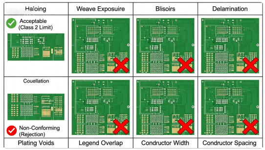
What Is an LED PCB? Ultimate Guide to PCB LED Design & Manufacturing
An LED PCB is a specialized printed circuit board designed for LED applications, delivering electric
In the world of PCB/PCBA manufacturing, the choice between leaded solder and lead-free solder is not just technical — it has profound implications for quality, reliability, cost, and regulatory compliance. For companies operating in North America and Europe, environmental mandates such as RoHS and REACH push many toward lead-free solder, while legacy applications or high-reliability industries may still prefer leaded alloys.
At HCJMPCBA, we understand that selecting the right solder material (especially lead free solder material) is critical. It affects process design, reflow profiles, joint integrity, and long-term performance. In this article, we will explain exactly what leaded and lead-free solder are, compare their differences, and — importantly — give you six practical ways to distinguish them. Whether you are an OEM engineer, procurement specialist, or a cross-industry buyer, this guide will help you make informed decisions about the solder used on your PCBA assemblies.
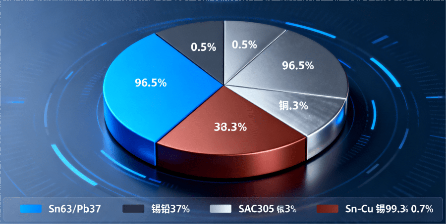
Leaded solder traditionally refers to tin-lead (Sn–Pb) alloys. The most common eutectic solder is Sn63/Pb37 (63% tin, 37% lead), which melts sharply at a single temperature. This composition has been the backbone of PCB assembly for decades because of its maturity, reliability, and favorable processing characteristics.
Other classic ratios exist (such as Sn60/Pb40), but Sn63/Pb37 remains widely used due to its ideal melting behavior.
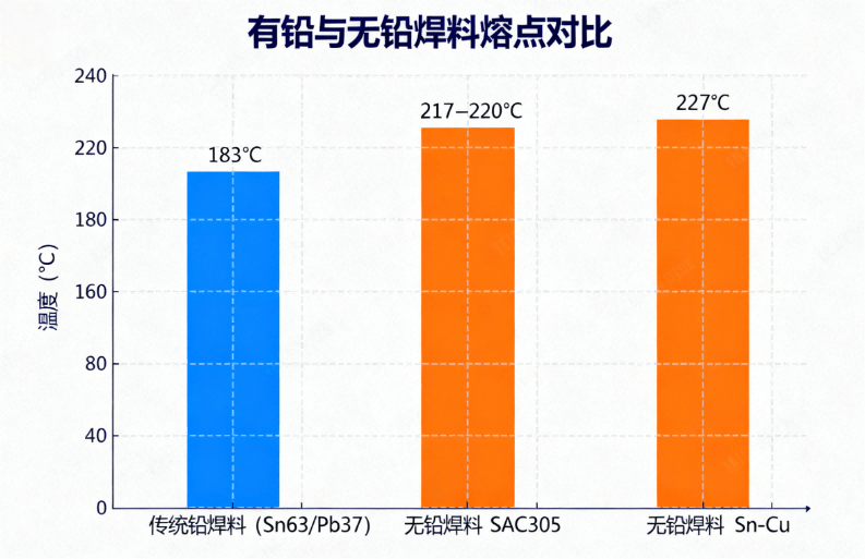
Melting Point: The eutectic Sn63/Pb37 alloy has a melting point of approximately 183 °C.
Wettability: Leaded solder generally offers excellent wetting behavior on metallic surfaces, which supports strong and reliable solder joints.
Mechanical Strength: Because of its composition, leaded solder is relatively soft, which can absorb stress well, but may be less strong in certain fatigue or high-stress scenarios.
Hcjmpcba Lead Vs Lead Free Solder Alloy Diagram
Leaded solder continues to be used in contexts where its advantages outweigh its environmental drawbacks:
Legacy or repair systems (old electronics, legacy aerospace, industrial machinery)
Prototyping and rework, where ease of use and lower melting temperatures are beneficial
Applications where RoHS or lead restriction is not required, or where high reliability under thermal cycling is less critical
Lead-free solder is typically based on tin (Sn) combined with other non-lead metals like silver (Ag), copper (Cu), bismuth (Bi), zinc (Zn), indium (In), or antimony (Sb).
Some of the most widely used lead-free solder alloys include:
SAC305 (Sn96.5 / Ag3.0 / Cu0.5) — very common in modern PCB assembly
Sn–Cu (e.g., Sn99.3 / Cu0.7) — lower cost lead-free
Sn–Bi (for low-temperature soldering)
Melting Point: Lead-free solders typically have higher melting points than leaded ones. For SAC305, the melting range is around 217–220°C.
Conductivity: Electrical conductivity may differ depending on alloy; some lead-free alloys may have slightly lower conductivity than Sn–Pb, but they are engineered to maintain good performance.
Corrosion Resistance & Thermal Stability: Many lead-free alloys show good resistance to thermal fatigue, and improved mechanical strength under cyclic thermal stress.
Lead-free solder is now standard in many industries, especially in markets where environmental compliance is mandatory:
Consumer Electronics: Smartphones, laptops, and household electronics
Automotive Electronics: ECUs, sensors, modules requiring long-term reliability under thermal cycling
Medical Devices: High reliability and compliance with international safety regulations
Industrial and IoT Devices: Where compliance and long-term performance are equally important
Here we break down the major differences in terms of chemistry, performance, and compliance.
Leaded solder: Contains a significant percentage of lead (Pb) — e.g., Sn63Pb37.
Lead-free solder: No lead; uses alloys like Sn-Ag-Cu, Sn-Cu, or Sn-Bi.
Melting Point: Leaded (Sn63/Pb37) ~ 183°C vs lead-free (e.g., SAC305) ~ 217–220°C
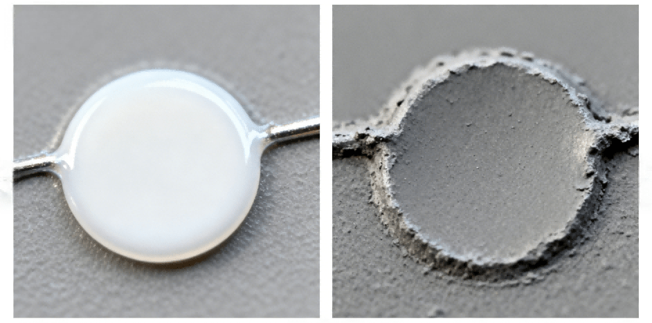
Color / Appearance: Leaded joints often appear bright and shiny, whereas lead-free joints may have a duller, matte finish.
Hardness: Lead-free solder joints are typically harder / more rigid than leaded ones, which can affect mechanical stress behavior.
Wettability: Leaded solder usually wets better, making it easier to form clean joints. In contrast, many lead-free alloys require more active flux or optimized reflow profiles to achieve comparable wetting.
Joint Reliability: Lead-free solders can form robust intermetallic compounds; under thermal cycling they often show good fatigue resistance — but this depends on alloy and process control.
Service Life: In many applications, properly processed lead-free joints can match or exceed the durability of leaded ones when designing for long-term use.
Regulatory Compliance: Lead (Pb) is restricted by RoHS (Restriction of Hazardous Substances) in Europe and many other markets.
Toxicity: Lead is a toxic heavy metal; eliminating lead reduces health risk for workers and end users.
Sustainability: Lead-free solder supports more sustainable, environmentally friendly manufacturing.
For quality control, procurement, or engineering teams, being able to verify whether solder is leaded or lead-free is essential. Here are six methods HCJMPCBA recommends:
Look at the color and sheen of solder joints: leaded solder tends to produce bright, shiny joints; lead-free often has a more matte or dull finish.
Surface texture can also hint at composition: if joints look grainy or dull, they may be lead-free.
Use a temperature-controlled hot plate or reflow oven with a thermocouple to test melting behavior.
If the solder liquefies around 183 °C, it’s very likely a classic leaded eutectic alloy (e.g., Sn63Pb37).
If it melts closer to 217–220 °C (or higher, depending on the alloy), it’s likely lead-free, especially common alloys like SAC305.
Hcjmpcba Melting Point Comparison Chart
Use X-ray fluorescence (XRF) equipment to detect and quantify lead (Pb) in the solder.
Alternatively, use lab-based alloy analysis to confirm the presence of tin, silver, copper, bismuth, etc. This is the most reliable method for confirming the exact alloy composition.
Examine solder wire or solder paste packaging: check for RoHS logos, alloy designations (e.g., “SAC305”, “Sn63/Pb37”), and any certification labels.
Manufacturers should clearly label the alloy; if it says SAC or “Pb-free,” that strongly indicates a lead-free solder.
Perform a test soldering run (e.g., reflow, hand soldering) and compare how the solder spreads and wets the PCB pads.
Lead-free solder often requires a slightly different process (more active flux, modified temperature profile) to achieve good wetting and minimize defects.
Use a microhardness tester or other mechanical test (shear, fatigue) to assess the joint’s hardness.
Lead-free joints tend to be harder and less ductile than leaded ones, which can be a clue.
For on-site, even a simple scratch test (if safe and appropriate) can sometimes give an indication — though lab tests are recommended for accurate results.
Choosing between leaded and lead-free solder isn’t always straightforward. Here are strategic guidelines based on use case.
Legacy Systems & Repairs: For maintenance of older electronics, where lead compliance isn’t required, leaded solder can offer ease of use and lower thermal stress.
High-Reliability or Niche Environments: In aerospace, military, or industrial applications where certification or specific mechanical behavior may favor leaded solder.
Prototyping & Development: For quick prototyping or debugging, leaded solder’s lower melting point and better flow may save time and reduce risk of damage.
Consumer & Commercial Electronics: Devices that need to comply with RoHS, REACH, or other environmental standards.
Automotive: Automotive ECUs, sensors, and modules that undergo thermal cycling benefit from robust lead-free alloys (e.g., SAC series).
Medical Devices: Where patient safety and regulatory compliance demand lead-free materials.
Sustainable / Green Electronics: For companies prioritizing environmental responsibility, lead-free solder is the clear choice.
Even seasoned professionals sometimes misunderstand aspects of leaded vs lead-free solder. Here are some common misconceptions, and clarifications:
“Lead-free solder is always worse than leaded.”
Not necessarily. Modern lead-free alloys (e.g., SAC305) often perform very well and, with correct process optimization, match or exceed reliability.
“You can freely mix leaded and lead-free solder.”
This is risky. Mixing can alter the alloy composition, change melting behavior, and potentially degrade joint quality.
“Higher melting point always means less reliable.”
While higher temperatures pose challenges, proper thermal profile control and flux chemistry can mitigate risks.
“Lead-free always cracks or corrodes more.”
It depends on the alloy. Some lead-free solders are engineered for high fatigue life and robust performance under thermal cycling.
Hcjmpcba Solder Joint Appearance Photo
Here’s how HCJMPCBA brings value to customers when it comes to solder selection and process control:
| Parameter | HCJMPCBA Capability | Customer Benefit |
|---|---|---|
| Alloy Support | Sn63/Pb37, SAC305, Sn99.3Cu, etc. | Flexibility for both legacy and RoHS-compliant assemblies |
| Reflow Profile Expertise | Optimized oven settings & thermal profiling | Reliable joint formation and minimized defects |
| Alloy Verification | In-house XRF or lab chemical analysis | Prevents cross-contamination and ensures correct solder usage |
| Mechanical Testing | Hardness, shear/fatigue tests | Assured reliability tailored to application |
| Regulatory Compliance | RoHS / REACH documentation and support | Easier certification and documentation for EU / NA customers |
| Technical Support | Process advice, flux recommendations, training | Tailored guidance for leaded or lead-free solder adoption |
Here are a few real-world scenarios in which HCJMPCBA has successfully implemented leaded or lead-free solder strategies:
Consumer Electronics
A North American OEM needed RoHS-compliant assemblies for a consumer device. HCJMPCBA used SAC305 lead-free solder and optimized the reflow profile, achieving reliable, glossy joints and full regulatory compliance.
Automotive Electronics Module
For a European automotive supplier, HCJMPCBA deployed a Sn99.3Cu lead-free alloy. The higher melting point was accommodated by our thermal profiling, and the parts passed rigorous thermal cycling tests.
Medical Device PCB
A medical equipment manufacturer required both lead-free solder and high joint reliability. HCJMPCBA performed in-depth mechanical testing (fatigue, shear) on SAC-based joints, ensuring they met long-term safety and performance standards.
Repair of Legacy Industrial Equipment
An industrial client had older control boards that were originally assembled with Sn63/Pb37. HCJMPCBA continued to support these with leaded solder to maintain material compatibility and ease of maintenance.
Choosing HCJMPCBA for your PCB / PCBA assembly means partnering with a company that:
Has deep expertise in both leaded and lead-free soldering.
Maintains strict quality control: alloy verification, mechanical testing, and process consistency.
Supports regulatory compliance (RoHS, REACH) for European and North American markets.
Offers process flexibility: we can adjust solder, flux, reflow, and rework to meet your needs.
Provides technical consultation to help you decide which solder is best for your application, and how to validate it.
Q: Is lead-free solder always more expensive than leaded?
A: Generally yes, because many lead-free alloys require silver or other expensive metals. But the cost can be offset by regulatory compliance, lower health risk, and long-term reliability benefits.
Q: Does lead-free solder damage temperature-sensitive components?
A: It can, due to its higher melting point, which demands higher reflow temperatures. However, with proper thermal profiling and careful flux selection, many sensitive components can be soldered reliably.
Q: Can I mix leaded and lead-free solder on the same board?
A: It’s not recommended. Mixed alloys can behave unpredictably, altering melting points and joint properties, potentially reducing reliability.
In summary:
Leaded solder (e.g., Sn63/Pb37) is well-established, easy to work with, and has a low melting point (~183 °C), but it carries environmental and health risks.
Lead-free solder (e.g., SAC305, Sn–Cu, Sn–Bi) uses tin-based alloys, has a higher melting point (~217–220°C for SAC305), and supports regulatory compliance while offering robust performance.
There are six practical ways to tell them apart: visual inspection, melting point test, chemical analysis, packaging verification, wettability behavior, and hardness testing.
The right choice depends on your application needs (legacy vs RoHS), process capability, and long-term reliability goals.
At HCJMPCBA, we bring world-class expertise in both leaded and lead-free solder assembly, backed by quality control and regulatory know-how. We help you choose the right soldering strategy, validate it, and deliver high-reliability PCBAs.
Call to Action (CTA):
Ready to optimize your PCB / PCBA assembly process with the right solder material? Request a Quote now from HCJMPCBA and discover how our expertise in leaded and lead-free soldering can improve your yield and compliance.
See Our Case Studies to explore how we’ve helped other clients succeed.
An LED PCB is a specialized printed circuit board designed for LED applications, delivering electric
The industrial control board PCBA as the core component of industrial control, its characteristics i
This article analyzes the future trends of the electronic manufacturing industry, including technolo