How to Use a Multimeter: The Complete Practical Guide for Engineers and Beginners
If you want to quickly understand how to use a multimeter, this guide explains the practical steps u
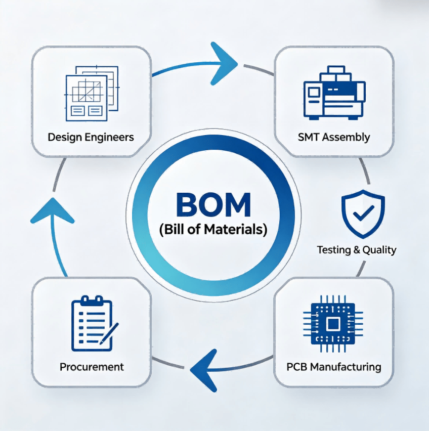
When global OEM engineers, procurement decision-makers, and end customers search for pcb manufacturing, they’re rarely looking for “just theory.” They want a predictable way to get reliable printed circuit boards—on time, to spec, and with minimal rework. In industrial programs, the difference between a stable product and a costly delay often comes down to whether the pcb manufacturing process is controlled with the right engineering checks, process discipline, and verification data.
This article explains the 12 steps in the pcb manufacturing process in a practical way, including common defects, buyer-friendly questions, and quality gates used in industrial pcb production and industrial pcb manufacturing. It also clarifies where PCB assembly (PCBA) fits in, and how to choose a supplier without hidden risk—especially if you build industrial control, military, communications, AI-related electronics, or low-altitude products that demand high reliability.
PCB manufacturing produces the bare board—layers, copper traces, holes, solder mask, and surface finish. It determines critical electrical and mechanical quality: trace geometry, hole wall integrity, impedance stability (if required), and long-term reliability of the base structure.
PCB assembly (PCBA) is the next stage: soldering components onto the finished board (SMT/THT), plus inspections like 3D SPI and 3D AOI, and validation such as X-RAY for hidden joints (e.g., BGA/QFN). A common sourcing risk is treating PCB fabrication and PCBA as unrelated—yet defects often “echo” across both stages. For example, a marginal via wall from the pcb fabrication process can become an intermittent failure after thermal cycling in assembly.
Practical advice: If you’re buying both, choose a supplier or supply chain that can connect the data: DFM feedback → fabrication controls → assembly controls → test reports. That’s how top industrial programs reduce rework and shorten launch timelines.
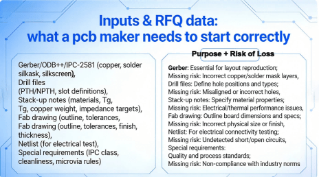
A professional pcb maker typically needs:
Gerber / ODB++ / IPC-2581 (copper, solder mask, silkscreen)
Drill files (PTH/NPTH, slot definitions)
Stack-up notes (materials, Tg, copper weight, impedance targets if any)
Fab drawing (outline, tolerances, finish, thickness, special notes)
Netlist (for electrical test matching)
Special requirements (IPC class target, cleanliness, microvia rules, etc.)
For stable industrial pcb manufacturing, RFQ clarity matters more than “lowest price.” A good RFQ calls out:
Quantity tiers (prototype / pilot / mass production)
Delivery expectations and whether you need partial shipments
Layer count, board thickness, copper weight, and controlled impedance needs
Surface finish choice (ENIG, OSP, HASL, immersion silver, etc.)
Hole types: microvia, via-in-pad (if applicable), backdrill, filled vias
Acceptance criteria (IPC-A-600 / IPC-6012 class if required by your program)
Special reliability needs: high-temp materials, CAF mitigation, thermal stress testing expectations
Many schedule slips begin with missing or ambiguous inputs:
No netlist → weak electrical test definition
Unspecified impedance → layout may not meet signal integrity
Undefined via structures → plating risk and assembly reliability issues
Unclear tolerances → mechanical fit issues at final enclosure integration
HCJMPCBA’s approach is to treat RFQ as an engineering handshake, not just a price request: DFM questions are raised early, and risk points are documented before release to production.
Pcb Manufacturing Rfq Information List Infographic
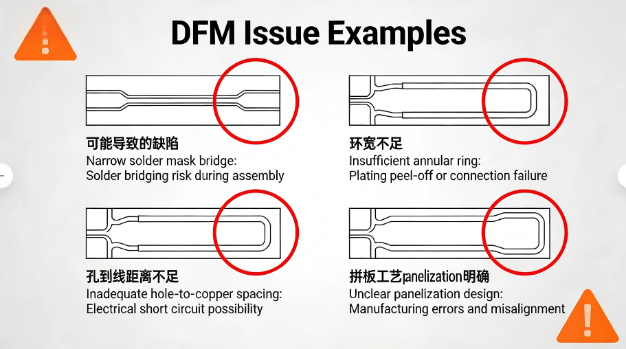
Pcb Manufacturing Example Diagram Of Dfm Issues
What happens: Engineering reviews your files for manufacturability (DFM) and testability (DFT), then CAM checks ensure layers align, drill maps are consistent, and manufacturing outputs are correct.
Key quality gate: DFM notes + CAM output verification.
Typical defects prevented: Wrong drill sizes, missing solder mask openings, incorrect layer polarity, panelization mistakes.
Buyer questions:
Do you provide a written DFM report and ECO/ECN control?
How fast is the DFM turnaround for prototypes?
This step is the “insurance policy” of the pcb manufacturing process—especially when designs are tight, multilayer, or intended for industrial pcb production where downtime is expensive.
What happens: Choose laminate system (e.g., FR-4 variants, high-Tg, low-loss materials) and finalize stack-up: dielectric thicknesses, copper weights, and—if needed—impedance targets and tolerances.
Key quality gate: Stack-up confirmation with measurable requirements (thickness, Tg, impedance notes).
Typical defects prevented: Warpage, impedance drift, delamination, unexpected signal loss.
Buyer questions:
Which materials are used and are they traceable by lot?
If impedance is required, what’s the control method and reporting?
For industrial control, military, communications, and AI hardware, material choice is often a reliability decision as much as a cost decision in industrial pcb manufacturing.
What happens: Copper on the inner layers is patterned using photoresist exposure (LDI or film) and etched to form traces—this is where the inner pcb circuit is created.
Key quality gate: Imaging alignment control + etching process stability.
Typical defects prevented: Over-etch (thin traces), under-etch (shorts), trace width variation.
Buyer questions:
What is the minimum line/space capability for production vs prototype?
How do you control critical trace geometry?
This stage is central to “manufacturing printed circuit” quality: if the geometry is unstable here, later steps can’t fully recover it.
What happens: AOI checks the inner layers for opens/shorts and pattern defects. Then surface treatment (often oxidation / alternative bonding treatment) prepares copper for lamination bonding.
Key quality gate: AOI pass criteria + defect classification (repair vs scrap).
Typical defects prevented: Hidden inner-layer shorts, open traces, nicks, copper anomalies.
Buyer questions:
Is inner-layer AOI standard for all multilayers?
How are defects recorded and traced?
In robust industrial pcb production, this is where many “silent failures” are caught early, before lamination hides them forever.
What happens: Inner layers are stacked with prepreg and outer copper foils, then pressed under heat and pressure to form a solid multilayer panel.
Key quality gate: Registration/alignment + lamination cycle control (temperature, pressure, time).
Typical defects prevented: Layer misregistration, resin voids, delamination, excessive warp.
Buyer questions:
What’s the warp/twist control method and acceptance criteria?
How do you handle tight registration requirements?
Lamination is often the “point of no return” in the pcb board manufacturing process—a disciplined press process prevents latent reliability problems.
What happens: Holes are created for vias and component leads. Advanced designs may require laser microvias, controlled depth drilling, or special slot routing.
Key quality gate: Drill accuracy + hole wall integrity + correct PTH/NPTH mapping.
Typical defects prevented: Broken drills causing rough walls, off-location holes, missing holes.
Buyer questions:
How do you verify drill quality (tool wear control, hole wall checks)?
Can you support microvias or special via structures if needed?
This step shapes the future reliability of plated holes—the backbone of many printed circuit boards used in harsh environments.
What happens: Desmear removes resin smear from drilling so plating can adhere. Then copper plating builds conductive barrels in holes and adds copper thickness to surfaces.
Key quality gate: Plating thickness control + adhesion verification.
Typical defects prevented: Thin barrel copper, voids, poor adhesion, intermittent connectivity after thermal stress.
Buyer questions:
What’s the target hole copper thickness?
Do you have process controls for high-reliability builds?
For industrial control, military, communications, and AI platforms, via reliability is a major risk driver. A controlled plating process is non-negotiable in industrial pcb manufacturing process work.
What happens: The outer copper layers are patterned and etched to form final traces and pads.
Key quality gate: Outer AOI (where applicable) + critical dimension control.
Typical defects prevented: Shorts between fine features, opens, pad geometry issues that harm assembly yield.
Buyer questions:
How do you control outer-layer trace width for consistency?
What inspection catches outer-layer shorts/opens?
This step is where “circuit board manufacturing” meets assembly reality: pad geometry must support stable soldering later.
What happens: Solder mask is applied, imaged, and cured to protect copper and define solderable areas.
Key quality gate: Solder mask alignment + thickness and cure control.
Typical defects prevented: Solder bridging, exposed copper corrosion, mask lifting or bubbles.
Buyer questions:
What’s your alignment control for fine-pitch designs?
Do you record mask-related defects and corrective actions?
In printed circuit board manufacturing process control, solder mask is both protection and assembly yield insurance.
What happens: Exposed copper pads receive a surface finish to protect from oxidation and enable soldering.
Key quality gate: Finish thickness/coverage + solderability considerations.
Typical defects prevented: Oxidation, poor solderability, premature pad degradation.
Buyer questions:
Which finish matches the storage time and assembly method?
Are there special reliability considerations for my environment?
Common selection logic (simplified):
ENIG: great planarity for fine pitch, good shelf life; higher cost
OSP: cost-effective, good for fast-turn; shelf-life and handling sensitivity
HASL: robust, often economical; less planar for very fine pitch
Immersion silver/tin: good solderability; storage and handling requirements vary
A mature pcb maker will help you choose based on assembly technology, product life, and total cost of risk—not just unit price.
What happens: Boards are routed or V-cut from the panel, edges are cleaned, and mechanical requirements are verified.
Key quality gate: Dimensional inspection + edge quality (no burrs that cause shorts or assembly damage).
Typical defects prevented: Out-of-tolerance outlines, edge burr shorts, connector fit issues.
Buyer questions:
What are the outline tolerances and inspection method?
How do you prevent edge-related shorts for dense designs?
This is often overlooked in “pcb process” discussions, yet mechanical problems can stop production instantly.
What happens: Electrical testing (flying probe or fixture) verifies continuity and isolation versus netlist. Final inspection checks appearance, markings, and packaging.
Key quality gate: Electrical test yield + inspection records + packaging standard.
Typical defects prevented: Shipping boards with opens/shorts, mixed revisions, handling damage.
Buyer questions:
Do you provide electrical test coverage for every shipment?
What shipping documentation is included (COC, test summary, traceability)?
This final gate is a core reliability promise in pcb manufacturing—and it’s where buyer confidence should be backed by data, not assumptions.
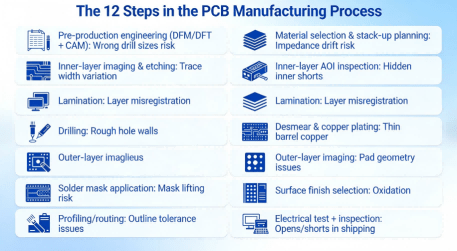
Overview Of The 12 Step Pcb Manufacturing Process
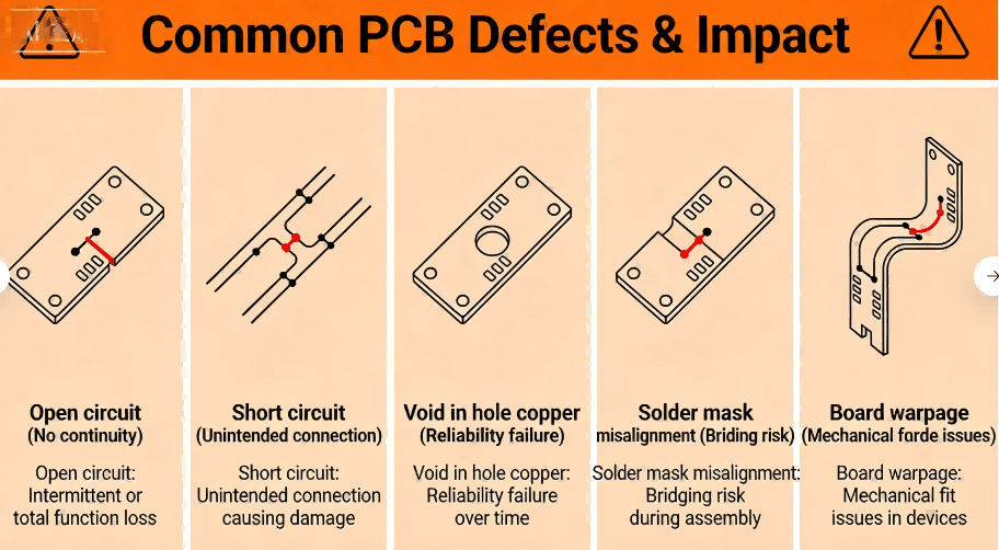
Pcb Manufacturing Process Comparison Diagram Of Defect Schematic Diagrams
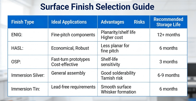
Pcb Manufacturing Process Surface Treatment Options
Industrial programs don’t just fail from “big mistakes.” They fail from small, repeated variations that accumulate: trace geometry drift, plating instability, solder mask misalignment, or revision confusion. That’s why mature industrial pcb production relies on quality gates—structured checkpoints where defects are caught early and recorded with traceability.
Depending on complexity and reliability class, buyers should look for:
Inner-layer AOI (for multilayers)
Outer-layer inspection/AOI (as applicable)
Plating thickness controls (hole wall reliability)
Dimensional checks after profiling
Electrical test vs netlist (flying probe/fixture)
Final inspection + packaging controls
For PCBA, critical inspection layers add:
3D SPI for solder paste volume/shape
3D AOI for placement and solder joint appearance
X-RAY for hidden joints (BGA/QFN/LGA)
IQC/IPQC/OQC to control incoming material, in-process quality, and outgoing quality
Ask what documentation is available with each shipment:
Certificate of Conformance (COC)
Electrical test summary and yield
Process inspection records (as needed by program)
Traceability identifiers (work order, lot, date code)
Change control record (ECO/ECN if revisions occur)
This evidence turns sourcing from “trust-based” to “data-based,” which is the most effective way to protect total cost in industrial pcb manufacturing.
The biggest cost drivers in pcb manufacturing and pcb board fabrication include:
Layer count and registration difficulty
HDI features: microvias, via-in-pad, filling/capping
Controlled impedance requirements
Copper weight and plating requirements
Surface finish selection
Testing coverage and reliability documentation
Material selection (high-Tg, low-loss, specialty laminates)
A low quote can be legitimate—or it can hide missing controls. Buyers should compare “apples-to-apples” using a structured checklist.
Fast-turn builds are valuable for prototyping, but they can increase risk if:
Engineering review is rushed
Material substitutions happen without approval
Inspection or electrical test coverage is reduced
If your program is industrial control, military, communications, AI hardware, or low-altitude applications, time-to-market matters—but so does stability. The best suppliers accelerate by improving engineering and process discipline, not by skipping gates.
Same layer count, thickness, copper weight, and finish?
Same test coverage (netlist-based electrical test)?
Same acceptance criteria (IPC class targets if required)?
Same panelization/array rules?
Same documentation and traceability commitments?
Same packaging method (ESD protection, vacuum packing if needed)?
HCJMPCBA supports a structured workflow designed for predictable outcomes:
RFQ intake with engineering clarification
DFM/DFT review and manufacturability feedback
Quote confirmation aligned with build rules and requirements
Prototype/pilot build with controlled release
Production ramp with traceability and quality gates
Shipment with inspection records and agreed documentation
This approach is built to reduce surprises in both pcb manufacturing and downstream PCBA.
For high-reliability programs, quality must be systematic—not heroic. HCJMPCBA operates under:
ISO 13485 and ISO 9001 management systems (medical-grade and general quality discipline)
Inspection and control capabilities including 3D SPI, 3D AOI, X-RAY, plus IQC/IPQC/OQC checkpoints
A culture of traceability and process accountability to support industrial and regulated applications
These capabilities are especially relevant to customers building industrial control hardware, military-related electronics programs, communications systems, AI-oriented electronics, and low-altitude products where reliability and consistency are critical.
“Fast” should come from:
Rapid, structured DFM feedback
Clear RFQ inputs and quick clarifications
Stable, repeatable process windows
Proactive risk identification before production
Not from reducing inspections or skipping verification.
What are the stable production capabilities (line/space, drill, layer count)?
Can you support my reliability target (IPC class expectations, traceability)?
What materials are standard—and can you support high-Tg/low-loss?
Can you provide the finish and shelf-life my assembly needs?
Are inner layers inspected (AOI) for multilayers?
What’s the plating thickness target and control method?
Is electrical test performed on 100% of boards?
What documentation comes with shipment (COC, test results, traceability)?
How quickly do you return DFM comments?
How are spec conflicts resolved and recorded (ECO/ECN)?
Do you proactively flag risk areas (warp, impedance, via reliability)?
Do you have 3D SPI and 3D AOI for SMT process control?
Is X-RAY available for hidden joints (BGA/QFN)?
How do IQC/IPQC/OQC work—what do you measure and record?
What is your approach to root cause analysis and corrective actions if issues occur?
A supplier who answers these well is less likely to create hidden cost in the total pcb production process.
Prototype lead time depends on layer count, materials, finish, and test requirements. Industrial pcb production for complex multilayers typically takes longer than simple boards, especially when controlled impedance or special via structures are required. A reliable supplier explains lead-time drivers clearly instead of offering vague promises.
PCB fabrication (pcb manufacturing / pcb fabrication) creates the bare board. PCB assembly (PCBA) mounts and solders components onto it, then verifies quality using tools like 3D SPI, 3D AOI, and X-RAY. In many programs, the best results come from connecting the fabrication controls to the assembly controls.
Common root causes include weak DFM alignment, unstable imaging/etching control, drilling damage, poor plating integrity, solder mask misregistration, and insufficient electrical testing. These issues are best managed with structured quality gates throughout the circuit board manufacturing process.
It depends on assembly pitch, storage time, and reliability expectations. ENIG is often chosen for fine-pitch planarity and shelf life; OSP can be strong for fast-turn and cost; HASL is robust but less planar for ultra-fine pitch. A disciplined pcb maker will recommend based on your risk profile and assembly method, not just cost.
Send manufacturing-ready data: Gerber/ODB++/IPC-2581, drill files, stack-up notes, fab drawing, and netlist. Clear requirements for finish, thickness, impedance (if needed), and acceptance criteria help prevent delays and rework.
A dependable industrial pcb manufacturing process is not simply “12 steps on paper.” It’s 12 steps executed with consistent engineering review, controlled processes, and evidence-based inspection. When buyers understand the key gates—DFM/CAM, imaging/etching control, drilling and plating reliability, solder mask alignment, surface finish selection, and electrical testing—they can evaluate suppliers more fairly and reduce total sourcing risk.
For OEM engineers and procurement teams sourcing pcb manufacturing, pcb fabrication process, printed circuit board manufacturing process, and pcb assembly process work, the safest path is choosing partners who can explain what they control, how they verify it, and what documentation proves it—especially in industrial control, military, communications, AI hardware, and low-altitude products.
If you want to quickly understand how to use a multimeter, this guide explains the practical steps u
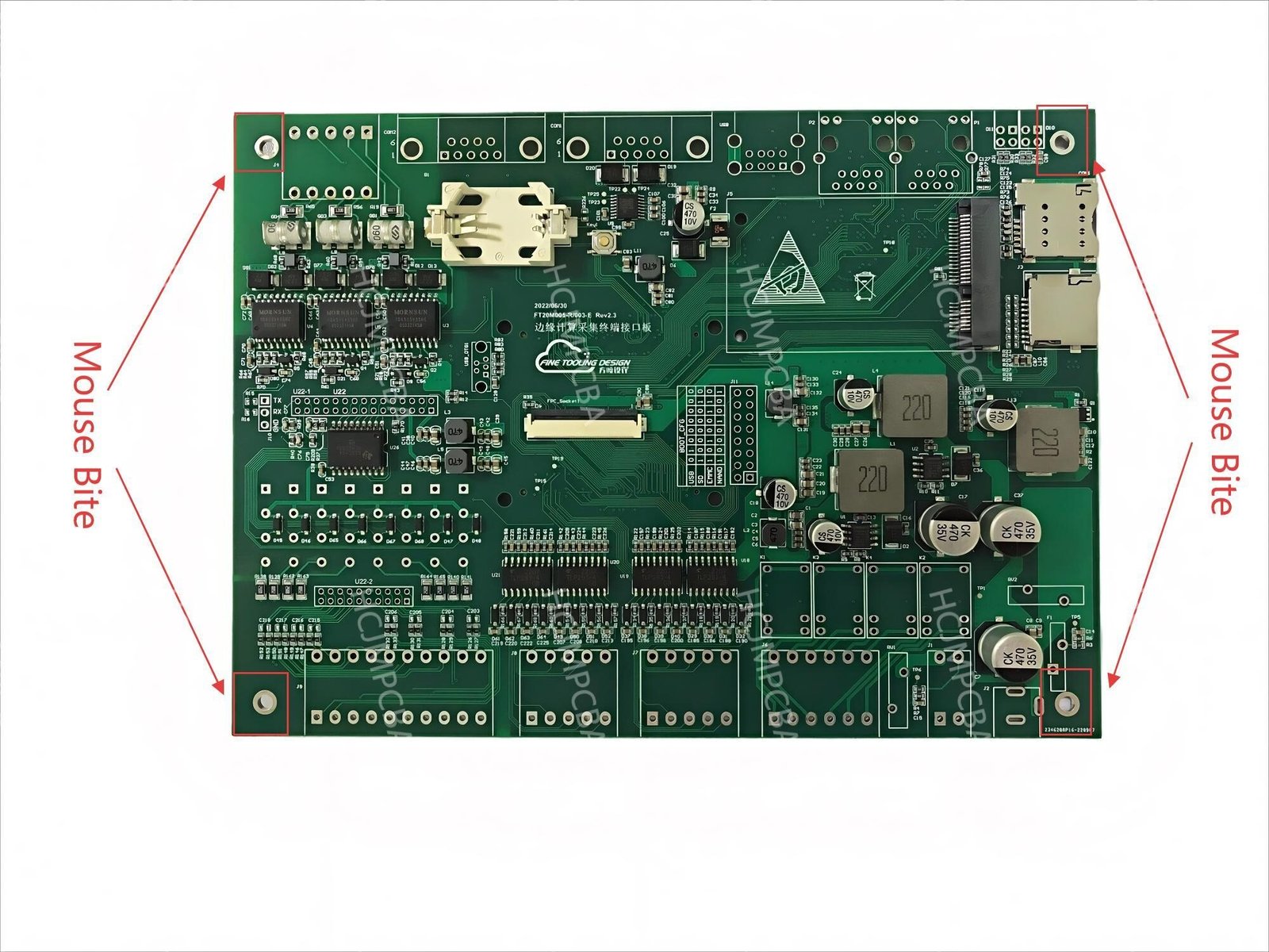
Curious what are mouse bites in PCB manufacturing? This comprehensive guide from HCJMPCBA explains m
Discover the essential distinction in pcb vs pcba. Learn what PCBA means, what is PCBA and its compo