10 Game‑Changing Steps to Flawless Custom PCB Design: From Cost Control to Cutting‑Edge Layouts
Discover a custom pcb design framework in 10 strategic steps—covering cost estimation, layout best
AOI Inspection PCB: 7 Powerful Insights into Automated Optical Inspection in PCB Manufacturing
Table of Contents
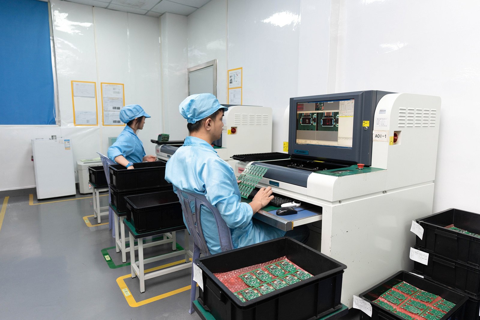
ToggleIn today’s electronics industry, printed circuit boards (PCBs) are becoming increasingly complex and miniaturized. Manual inspection simply cannot keep pace with the demand for speed, accuracy, and consistency. That’s where aoi inspection pcb—Automated Optical Inspection—becomes essential. It allows manufacturers to detect defects early in the process, ensuring high-quality output and reducing costly rework or recalls.

Automated Optical Inspection (AOI) is a non-contact inspection method that uses optical systems—cameras, lighting, and software—to scan PCBs or PCB assemblies (PCBAs) for defects. It replaces traditional visual checks by automatically identifying issues like missing components or solder defects. This technology can inspect both bare PCBs and assembled boards, at various stages such as post-reflow, enabling early detection of flaws and improving product reliability.
-Optical Hardware: High-resolution cameras, strategic lighting systems—LED arrays or structured light—that illuminate the board at multiple angles.
-Image Processing Software: Advanced algorithms compare captured images against reference (“golden”) boards to detect deviations.
-Motion Control: XYZ stages or conveyors move boards through inspection zones, ensuring full coverage.
-The AOI Workflow:
(1)Capture images of PCB.
(2)Analyze via software for defects such as misalignment or solder issues.
(3)Flag and report defects for rework.
This mechanism underlies aoi automated optical inspection, delivering speed, repeatability, and accuracy.
-2D AOI captures surface information—ideal for detecting component presence, alignment errors, and surface-level issues. However, shadows or reflections can cause false positives.
-3D AOI, by measuring height and volume, can detect hidden flaws like insufficient solder volume, lifted leads, or uneven joints. It provides greater accuracy and fewer false calls, especially for fine-pitch components.
| Feature | Description |
|---|---|
| High-speed inspection | Automatically scans hundreds of boards per hour with precision |
| Programmable lighting | Customizable illumination enhances defect visibility |
| Algorithm-based detection | Detects component misplacement, polarity errors, solder bridges, and more |
| Defect traceability | Records inspection images and logs for QA traceability |
| Versatility | Works in different production stages (pre/post-reflow, wave solder) |
These highlight the extensive capabilities of aoi inspection systems, making them indispensable within modern PCB assembly lines.
(1)Bare PCB Inspection
Detects manufacturing defects like shorts, missing pads, engraving errors, or copper excess.
(2)SMT / Assembly Inspection
Flags SMD misplacement, tombstoning, solder bridges, or orientation errors using aoi optical inspection.
(3)3D Inspection for Solder Joints
Measures solder volume and ensures uniformity—critical for reliability, especially under vibration or thermal stress.
(4)Post-Wave / Box Build Inspection
Validates through-hole soldering, component polarity, and overall mechanical assembly integrity.
(5)Industry-Specific Use Cases
Medical Devices: No room for failure—AOI ensures each board meets strict standards.
Automotive / Aerospace: Identifies minute defects affecting safety and performance.
(1)Increased Yield: Detects defects early, reducing waste and rework.
(2)Consistency: Automated systems provide uniform results across large production runs.
(3)Cost-effective: Saves time compared to manual inspection and reduces human error.
(4)Traceability: Logs inspection records for quality control and certification.
(5)Scalability: Supports ramp-up during high-volume or rapid-prototype production.
(1)Complexity in Programming: Accurate detection requires sophisticated setup and tuning.
(2)Upfront Cost: 3D AOI units are high-investment, though deliver ROI via improved yields.
(3)Detection Gaps: Hidden joints (e.g., under BGAs) or multi-layer internal issues may still require X-ray or ICT follow-up.
(1)Evaluate if suppliers use both 2D and 3D AOI inspection machines—especially relevant for high-reliability products.
(2)Verify AOI systems integrate traceability and detailed reporting.
(3)Ensure your manufacturing partner uses AOI across multiple stages (e.g., post-reflow).
(4)Prioritize those with experience in high-density, fine-pitch designs using aoi inspection systems.
(5)Ask for examples or case studies demonstrating reduction in defects or improved yields.
(1)AI-enhanced Algorithms: Reduces false positives and improves detection through machine learning.
(2)Industry 4.0 Integration: AOI connecting with MES systems for real-time quality monitoring.
(3)Faster 3D Scanning: New optics enable real-time high-precision inspection even at high throughput.
(4)Smart Data Analytics: AOI-generated data drives process improvements and preventive maintenance.
AOI is the backbone of quality control in modern electronic manufacturing. As PCBs become more complex and production demands rise, aoi inspection pcb ensures efficiency and reliability through automated, precise defect detection. Whether you are evaluating aoi inspection systems, aoi inspection machine options, or integrating 3D AOI, quality-conscious OEMs should prioritize suppliers with these advanced inspection capabilities.
To learn more about advanced PCBA services and AOI inspection solutions, please contact HCJMPCBA.
Discover a custom pcb design framework in 10 strategic steps—covering cost estimation, layout best
Discover what a gerber file is, why it is the universal “language” for PCB manufacturing, how to
HCJMPCBA offers high-performance BT PCB manufacturing using Bismaleimide-Triazine resin. Explore the