QFN Package with Lid: Definition, Types, Thermal Performance & How to Choose the Right PCBA Supplier
Discover what a QFN package with lid really means — its structure, advantages, thermal and electri
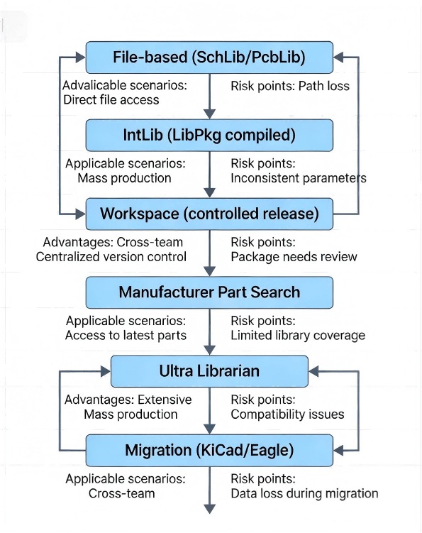
To master how to import component in altium, the safest approach is to import (or create) three linked assets—symbol, footprint, and 3D model—then validate mapping, parameters, and manufacturing layers before reuse. File-based libraries work for small teams, Integrated Libraries improve repeatability, and a Workspace enables governance. Vendor sources (Manufacturer Part Search or Ultra Librarian) can accelerate component create, but every imported part still needs verification of package, pin-1, polarity, rotation, and paste/courtyard rules.
Need speed for a prototype: file-based library import (SchLib/PcbLib) + local verification
Need repeatable builds: compile LibPkg → IntLib, then distribute the IntLib
Need team governance: publish to Workspace (managed components)
Need supply-chain linkage: Manufacturer Part Search (verify!)
Need vendor models: ultra librarian altium (verify mapping + land pattern)
Need migration: kicad to altium or Eagle import, sometimes via eaglecad to kicad as an intermediate
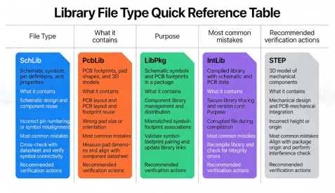
| Asset / file | Contains | Used for | Typical pitfalls |
|---|---|---|---|
| SchLib | Schematic symbols | import symbol, pin definitions | Wrong pin numbering, missing electrical types |
| PcbLib | Footprints (land patterns) | Pads, courtyards, assembly layers | Incorrect pad sizes, origin/rotation errors |
| STEP (3D) | 3D body geometry | Mechanical clearance checks | Wrong height/origin, missing keepouts |
| LibPkg | A package project referencing libs | Build pipeline for repeatability | Broken references when paths change |
| IntLib | Compiled integrated library | Easy distribution and version control | “Works on one PC only” if not compiled correctly |
Importing a component is often treated as a clerical EDA step. In reality, it is an early-stage quality gate that can prevent expensive downstream failures. A symbol that looks fine but maps to the wrong footprint can silently pass schematic review and only surface during assembly, when polarity is reversed, pads are undersized, or the placement origin is wrong. These issues can trigger rework, scrap, delayed shipments, and repeated engineering loops across time zones.
For global OEM engineering teams and procurement decision-makers, the risk is amplified by:
Mixed library sources (internal altium library, vendor downloads, legacy altium lib, and third-party portals)
Rapid supply-chain substitutions that change package variants
Inconsistent parameters (MPN, package, voltage ratings, approved alternates)
Cross-tool migrations (kicad to altium, Eagle conversions, legacy databases)
A stable library process reduces risk because it aligns the design intent (symbol + parameters) with manufacturability (footprint + assembly layers) and mechanical fit (STEP). The objective is not “having more parts,” but having trusted parts that can be reused without surprises.
what is electronic design automation? It is the set of tools and workflows used to design electronic systems—capturing schematics, laying out PCBs, checking rules, managing libraries, generating manufacturing outputs, and coordinating collaboration. In practice, electronic design automation determines how reliably a design moves from concept to manufacturable data.
In eda electronic design automation, component data is the “source of truth” that links:
Electrical intent (pins, nets, symbol)
Physical reality (footprint geometry and layers)
Mechanical constraints (3D body, height, keepouts)
Supply chain (MPN, alternates, lifecycle status)
Manufacturing/test requirements (polarity, orientation marks, test access)
Because of that linkage, electronic design automation software decisions are not only about routing features—they also affect library governance, traceability, and the ability to maintain consistent part definitions across teams.
A buyer may search phrases like “evaluate the electronic design automation company cadence on eda software,” to compare capabilities. A practical evaluation should focus on:
Library data integrity and change control
Collaboration and permissioning (who can edit a released component)
Interoperability and import/export robustness
Auditability: when and why a symbol/footprint changed
Integration with part data (MPN and alternates)
These criteria matter as much as routing speed when designs are handed to an EMS/PCBA partner at scale. (This same phrase—“evaluate the electronic design automation company cadence on eda software,”—shows up again later with a checklist.)
A strong import workflow starts with decisions that make parts reusable. Without these rules, every new import increases inconsistency, and the library becomes a liability.
A disciplined approach typically defines:
Symbol name (functional identity): e.g., “MCU_STM32F4xx_100pin”
Footprint name (physical identity): e.g., “LQFP-100_14x14_P0.5”
3D model name (mechanical identity): e.g., “LQFP100_14x14_H1.4”
Component create rule: what qualifies as “released” and reusable
Minimum parameters that help both engineering and purchasing:
MPN + manufacturer
Package / case code (altium package field)
RoHS/REACH notes if relevant to the project
Approved alternates (AVL entries)
Mount type, temperature grade where applicable
Polarity/orientation notes for assembly drawing
Treat each critical component as a controlled asset. A component project approach means:
A component has an owner and a review gate
Changes are logged and traceable (who changed pads, why)
Released parts are reused; experimental parts stay isolated
This prevents “silent edits” that cause manufacturing variation across builds.
The correct method depends on team size, collaboration, and risk tolerance. Every option can work—if verification is done correctly.
File-based import is common for prototypes and small teams:
Import a SchLib (symbol) and PcbLib (footprint)
Use a clear folder structure and lock released versions
This is the simplest form of library import, but it can become fragile if paths differ across PCs.
For repeatable builds, compile a LibPkg into an IntLib:
The IntLib bundles the assets
Teams can install a single file
This improves consistency and reduces missing-file issues.
For distributed teams, a Workspace enables:
Controlled publishing and revision history
Permissioning and release workflows
Standardized parameters for BOM integration
It is a strong solution when multiple engineers and sites contribute to the same altium libraries.
Manufacturer Part Search can accelerate part creation by pulling parametric data and sometimes footprints. It is useful for quick starts, but it still requires verification of land patterns, pin mapping, and package variants.
ultra librarian altium workflows often provide convenient symbol/footprint/3D bundles. This can reduce manual work on complex ICs and connectors. However, it must still be validated against datasheets and manufacturing rules (paste, courtyard, rotation marks).
When converting designs or libraries:
kicad to altium workflows may require re-checking layer mapping, footprints, and 3D orientation
Eagle conversions can be direct or involve intermediate steps like eaglecad to kicad before returning to Altium
Migration is feasible, but never assume imported footprints are production-ready without review.
This section provides a repeatable checklist that works whether the source is a vendor download, legacy altium lib, or a newly created part.
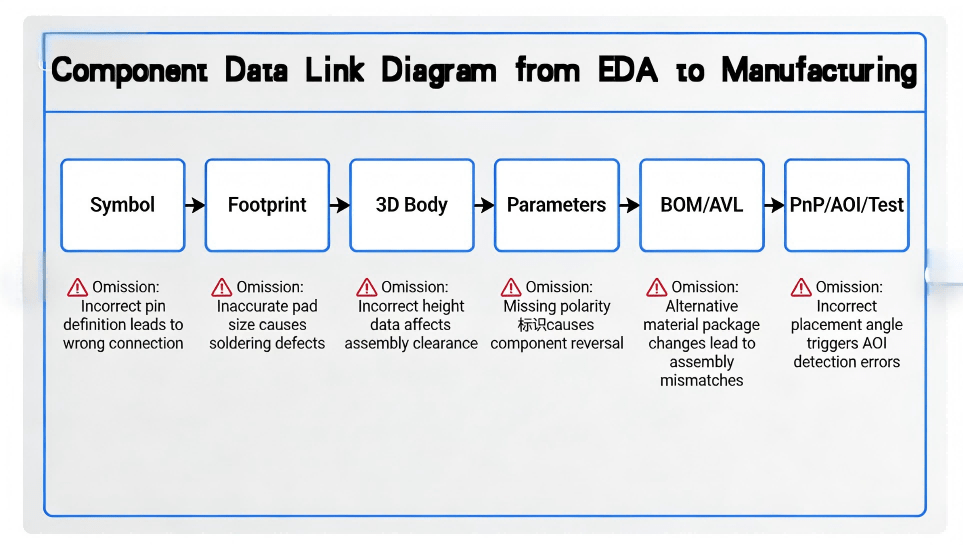
A complete component definition has four elements:
Symbol (SchLib): pins, electrical types, pin numbers
Footprint (PcbLib): pads, solder mask/paste, courtyards, assembly layers
3D model (STEP): mechanical shape and height
Parameters: MPN, description, altium package, alternates, notes
When someone asks how to import component in altium, the hidden failure mode is importing only the symbol or only the footprint.
For import symbol workflows:
Confirm pin numbers match the datasheet pinout (not only names)
Check electrical types (power input, passive, I/O) to reduce ERC noise
Verify special pins (thermal pad, exposed pad, shield pins)
After the import symbol step, do a quick sanity check: does the symbol reflect functional grouping (power pins, IO banks, differential pairs) to reduce schematic errors?
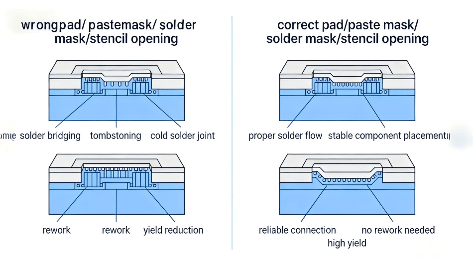
A footprint is where most production failures originate. Verification should include:
Pad size/shape and solder mask expansion
Paste mask aperture and stencil intent (especially for QFN/BGA)
Courtyard and assembly outline
Reference designator placement and readability
Placement origin (centroid) and rotation convention
This is where “looks okay” can still solder wrong, particularly for fine-pitch parts.
Mapping errors cause the worst surprises:
A correct symbol with the wrong footprint equals a wrong board
A correct footprint mapped to the wrong pin numbers equals functional failure
Ensure the component definition explicitly links:
Symbol pins ↔ footprint pads
Alternate footprints if package variants exist
This is the heart of robust library import—the mapping must be explicit and reviewed.
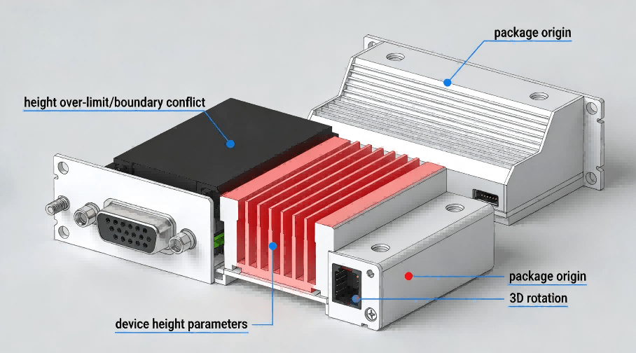
Mechanical fit issues often surface late. When attaching STEP:
Verify Z-height is correct (including standoffs, shields, tall electrolytics)
Confirm model origin matches footprint origin
Check rotation so pin-1 orientation is consistent
Run a simple collision review against enclosures, heatsinks, connectors
A correct STEP attachment strengthens the “digital thread” from PCB to mechanical integration.
A reusable part should carry enough data to reduce back-and-forth:
Manufacturer + MPN
Package field (use altium package consistently)
Notes on polarity/orientation
Approved alternates and lifecycle notes
This is where altium library data becomes procurement-friendly.
If the team needs stable distribution:
Place SchLib + PcbLib (and references) into a LibPkg
Compile to IntLib
Store and version it in a controlled repository
This step supports consistent builds across multiple engineers and sites.
For organizations that require governance:
Publish and release a managed component
Assign lifecycle state (draft → reviewed → released)
Restrict edits to prevent silent changes
This is often the best path when many projects share the same altium libraries.
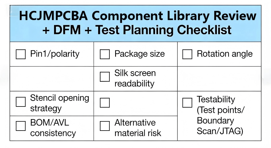
Before the part is reused in real products, validate:
Pin-1 and polarity marks (silkscreen + assembly)
Rotation convention across BOM, pick-and-place, and assembly drawing
Paste strategy for thermal pads (windowing if needed)
Courtyard for placement and rework clearance
Test access considerations (probe points, boundary scan pins)
This final step turns “imported” into “trusted.”
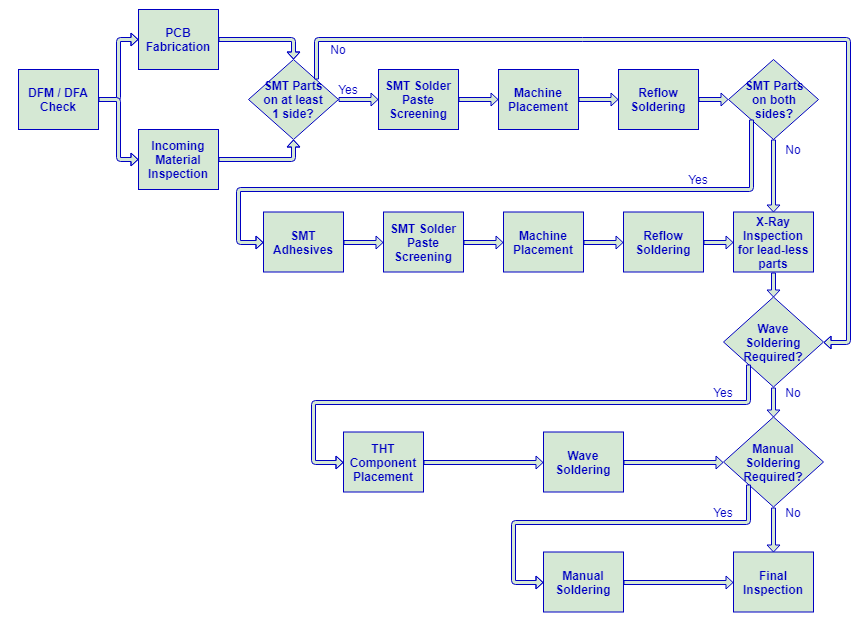
How To Import Component In Altium Decision Tree Flowchart
How To Import Component In Altium Quick Reference Table For Library File Types
How To Import Component In Altium Component Data Link Diagram
How To Import Component In Altium Comparison Of Package Errors
How To Import Component In Altium Hcjmpcba Component Library Review Dfm Test Planning Checklist
How To Import Component In Altium Example Of 3d Interference Check
Typical causes include:
Library not installed/added to search paths
File paths differ across machines (file-based altium libraries)
Conflicts between multiple versions of the same part
Fix approach:
Consolidate libraries into a controlled folder structure
Avoid duplicate names across altium lib sources
Prefer IntLib or Workspace publishing for distributed teams
Symptoms:
Symbol places fine, but PCB footprint is blank or “not found”
ECO fails or the PCB component has no pads
Fix approach:
Explicitly remap symbol models to the correct footprint
Verify pad numbering alignment (critical for ICs)
Re-check that the footprint is present in the same library set
This is common in kicad to altium conversions and legacy library imports:
mm ↔ mil mismatch
Origin placed at a corner instead of centroid
Rotation conventions not consistent with pick-and-place expectations
Fix approach:
Reset origin to the intended placement centroid
Standardize rotation reference (e.g., pin-1 indicator)
Run a placement preview and compare with assembly drawing conventions
When converting designs:
Courtyard or assembly outlines may land on unexpected layers
Text and reference designators may be lost or merged
This can happen when teams go from Eagle or eaglecad to kicad, then continue to kicad to altium.
Fix approach:
Rebuild courtyard and assembly layers using a consistent internal standard
Confirm solder mask/paste layers explicitly
Common reasons:
Overly aggressive paste apertures for fine pitch
Incorrect solder mask expansion
Thermal pad paste strategy not defined
Fix approach:
Adjust paste strategy (especially for QFN thermal pads)
Validate against datasheet land-pattern guidance and assembly constraints
For critical parts, run a small pilot build with inspection feedback
A scalable system typically includes:
One owner per released part
Review gate for footprint edits
A component project template: naming + parameters + mapping rules
Controlled release states (draft → reviewed → released)
Deprecation policy (do not delete; archive with notes)
This reduces library drift and prevents silent footprint changes that break manufacturing.
Third-party or vendor libraries are useful for speed, but verification is non-negotiable. A safe rule:
Trust the data source for pinout and parameters only after cross-check
Trust the footprint only after pad/courtyard/paste review
Trust the 3D only after origin/height verification
This applies to Manufacturer Part Search and ultra librarian altium alike. The workflow remains the same: import symbol, verify mapping, validate manufacturing layers, then release.
For each released part in an altium library, ensure at least:
MPN + manufacturer
Package name (consistent altium package usage)
Height (for mechanical constraints and packaging)
Polarity/orientation note for assembly
Approved alternates for sourcing resilience
This avoids repeated clarifications during procurement and PCBA quoting.
If multiple engineers and sites are involved:
Use IntLib for controlled distribution, or
Use Workspace publishing for auditability
Both approaches reduce the “works on one PC only” problem common in file-based altium libraries.
A component library is valuable only when it results in predictable assemblies and testable products. HCJMPCBA focuses on connecting EDA intent to manufacturable and testable outcomes—especially for customers who require specific verification beyond standard inspections.
A robust transfer from design to production often follows:
1.Library sanity-check: confirm imported components are consistent (symbol/footprint/3D/parameters)
2.BOM/AVL alignment: validate MPNs, package variants, alternates, and supply-chain feasibility
3.DFM review loop: check solderability risks, fine-pitch constraints, placement clearances, and assembly drawing clarity
4.Pilot build (if needed): build a small batch to validate real solder behavior and assembly constraints
5.Test plan finalization: implement inspection and test according to customer requirements
This is where component data quality, component create discipline, and test planning converge.
Many projects fail not because the PCB cannot be assembled, but because the verification strategy is unclear. HCJMPCBA emphasizes test readiness early and supports customer-defined test requirements, such as:
Clear definition of acceptance criteria and coverage (what must be verified, and why)
Fixture-based or fixtureless strategies depending on volume and product lifecycle
Test-point planning feedback (improves probe access and coverage)
Functional test (FCT) aligned to the end use case, including power-up sequences and I/O behavior
When customers provide a test specification, HCJMPCBA can implement the requested plan and align manufacturing outputs (BOM, assembly drawings, programming steps, test records) to match that specification.
Availability and selection depend on product type, density, and coverage goals, but typical approaches include:
Visual inspection and process checks
Automated optical inspection (AOI) for solder joints and placement
X-ray inspection for hidden joints (e.g., BGA/QFN) when required
In-circuit test concepts (ICT) or electrical continuity strategies, where applicable
Functional test (FCT) with customer-defined vectors and criteria
Programming and verification flows for MCUs or configurable devices
The key is not “more testing,” but appropriate testing that matches risk, volume, and customer requirements.
To reduce procurement uncertainty, a buyer can request:
A documented test plan and coverage statement
Clear definitions of pass/fail criteria and records retention
First-article review outputs (what changed between pilot and production)
Traceability expectations for critical components
Handling plan for substitutions (how alternates are proposed and approved)
This aligns with what many teams look for when they evaluate the electronic design automation company cadence on eda software, because both EDA systems and EMS partners are judged on traceability and controllability, not just convenience.
In everyday practice, altium package should be treated as a physical identity field that anchors footprint choice and assembly constraints. It is not just a label—when it changes, land pattern and sometimes 3D height/origin must be re-validated.
import symbol: ensures electrical correctness and connectivity
Footprint: ensures solderability and correct placement
STEP: ensures mechanical fit and assembly clearance
Missing any one of these increases risk.
These phrases commonly describe real-world data flows:
Some teams convert from Eagle to KiCad first (eaglecad to kicad) to standardize libraries
Then they migrate into Altium (kicad to altium) for enterprise workflows
In both transitions, layer mapping, origins, rotations, and courtyard rules require careful review.
electronic design automation: the discipline and toolchain
electronic design automation software: the tools used to implement it
eda electronic design automation: a common phrasing used in documentation and procurement
electronic design automation eda software: emphasizes both the category and software selection
Consistency in terms helps engineering and procurement teams communicate requirements clearly.
Many migrations are possible, but success depends on how clean the source libraries are. For kicad to altium, the critical checks are footprint origins, pad numbering, and layer mapping. For Eagle, direct import may work, but some teams use eaglecad to kicad as an intermediate step to normalize libraries. In all cases, imported footprints must be verified before production.
It is a strong starting point for parametric data and sometimes models, but production use still requires validation of land patterns, polarity/orientation, and package variants. Treat it as an accelerator—not a replacement for review.
ultra librarian altium is often useful for complex ICs and connectors because it can provide symbol, footprint, and 3D quickly. It is still essential to confirm pin mapping, pad geometry, paste strategy, and rotation conventions. For high-risk components, a pilot build plus inspection feedback is recommended.
Use a controlled component project process and prefer repeatable distribution (IntLib) or managed publishing (Workspace). Avoid multiple uncontrolled copies of the same altium lib across departments. Released parts should be treated as controlled assets.
Provide a written test specification that includes coverage goals, pass/fail criteria, any programming steps, and required records. If test points or access constraints exist, communicate them early so the design can support the test strategy. HCJMPCBA emphasizes implementing tests according to customer requirements and aligning production documentation to the agreed plan.
Import or create symbol and footprint
Attach STEP if mechanical fit matters
Verify mapping, pin-1, polarity, origin/rotation
Normalize key parameters (MPN, altium package, alternates)
Compile to IntLib or publish to Workspace
Implement a component project review gate
Standardize parameters and naming for all altium libraries
Define a repeatable validation checklist for every component create cycle
Discover what a QFN package with lid really means — its structure, advantages, thermal and electri
Discover a custom pcb design framework in 10 strategic steps—covering cost estimation, layout best
Guangzhou Huachuang Precision Technology Co., Ltd. has introduced intelligent feeder racks to provid