Design & Stack‑Up Planning
Plan layer count, copper weight, and substrate choice (e.g. FR‑4, ceramic pcb material, aluminium foil). Define ground/power planes and signal layers. Consider rigid vs flexible pcb board designs or high‑density stack-ups. Review with your multilayer pcb supplier for DFM compliance.
Inner‑Layer Imaging, Etching & Inspection
Each copper layer is imaged via laser UV exposure and etched to form circuit patterns. Automated optical inspection (AOI) is used to catch defects before lamination.
Lamination & Layer Alignment
Stack inner cores and prepreg under heat and pressure to bond the whole board. Alignment pins or fiducials ensure precise layer registration. This step repeats for blind/buried vias in HDI or aerospace designs.
Drilling & Via Formation
Use mechanical or X‑ray guided drilling for through-hole and microvias. Laser drilling enables high precision in dense boards like drone circuit board or aerospace pcb products.
Copper Plating & Surface Finish
Apply electroless copper inside drilled holes then plate panel to build thickness. Choose lead‑free solder compatible finish such as ENIG or HASL for long-term reliability and solderability.
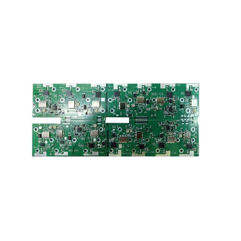
Outer‑Layer Imaging & Final Etching
Image the outer copper layers, remove resist, and etch away unwanted copper. Perform final DRC and visual inspection to ensure pattern accuracy.
Solder Mask, Silkscreen & Board Protection
Apply colored solder mask (common “purple circuit board” or green) to protect traces. Print silkscreen legends, date codes, or part identifiers. Optionally add pcb coating for moisture or chemical protection.
Routing, Depaneling & Profiling
Cut the production panel into individual boards using V‑scoring or CNC routing. Laser depaneling ensures minimal mechanical stress and clean edges.
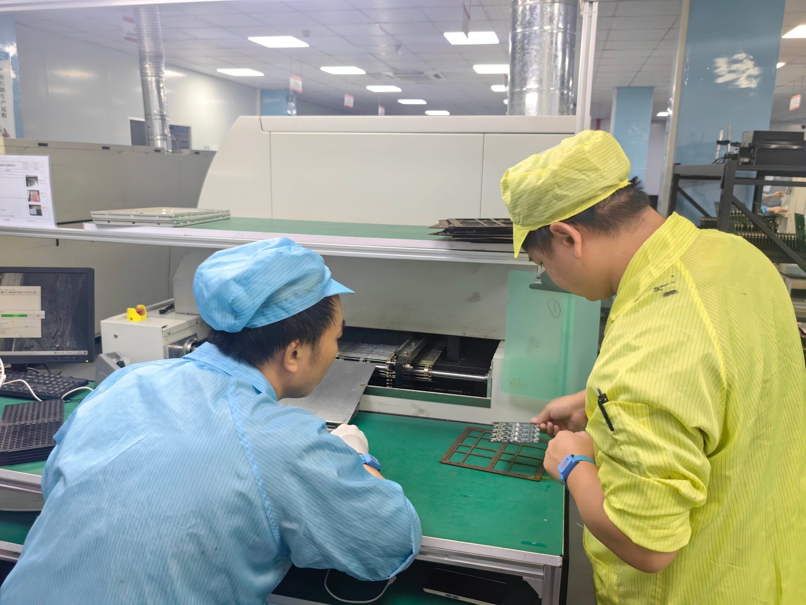
Electrical Testing & Quality Control
Bare‑board testing for continuity and isolation. Use pcb testing services, including flying probe or bed‑of‑nails fixtures. Functional tests verify complex boards before assembly.
Assembly & Final Inspection
DM: Though finished board production is outside fabrication, seamless transition to pcb board assembly and functional testing ensures your multilayer circuit board is ready for PCBA production.
Choosing Materials & Special Applications
-
For high-frequency or thermal applications, consider ceramic pcb board or ceramic pcb manufacturer
-
For lightweight or rigid-flex designs, evaluate aluminium pcb circuit board
-
Common use cases include drone pcb board, automotive, aerospace, and high-speed computing.
How to Select a Reliable Manufacturer To Priduce Multilayer Circuit Board
Look for capabilities in HDI, rigid-flex, lamination precision, clean-room operations, and multilayer manufacturing expertise. HCJMPCBA offers turnkey multilayer PCB fabrication, rigorous inspection protocols, and ISO-certified control.
Producing a multilayer circuit board involves intricate steps—from design and material selection to drilling, plating, coating, and testing. Each stage is essential to delivering reliable, high-performance boards.
To learn more about our PCBA services, please contact Guangzhou Huachuang Precision Technology (HCJMPCBA).