7 Proven Tips for Choosing the Best Automotive PCB Fabrication & Assembly Partner
Discover the 7 powerful strategies to evaluate and select the best Automotive PCB Fabrication & Asse
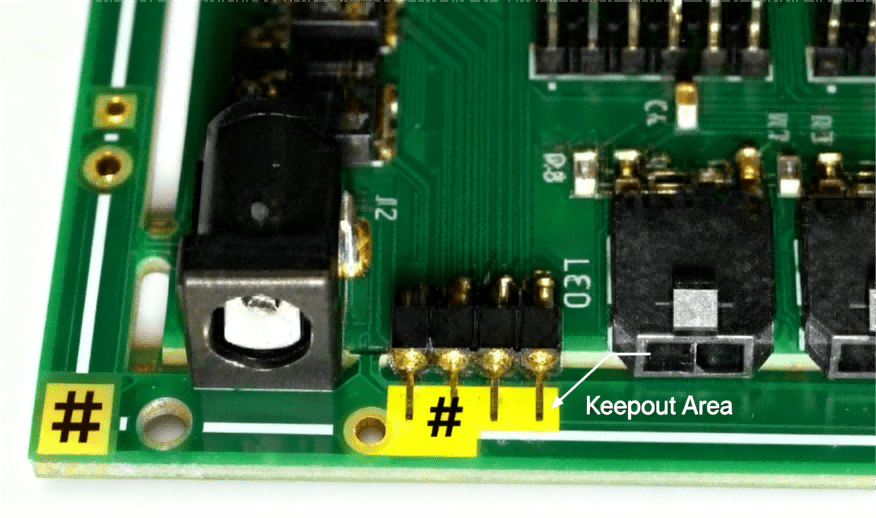
At its simplest, a keepout is a defined geometric area on a PCB layout (or footprint, or board-level rule) which disallows one or more categories of conductive items: copper traces, vias, pads, component bodies, or copper pours (zones). In other words, it’s a “no-go” zone for specific electrical / mechanical features.
Because it’s enforced by the EDA tool and tied into design rule checks (DRC), a keepout is more reliable than a textual note or annotation — it can prevent rule violations, catch them automatically, and communicate constraints across teams.
You’ll often see phrases like “keepout zone”, “outlayer” (less common), “keepout sign” (i.e. marking), or “board outline keepout”. In tools like Altium, the Keepout Layer is the standard mechanism for global exclusion, but you can also define layer-specific keepouts.
Keepout is sometimes confused or conflated with:
1.Board outline / mechanical outline layers: boundaries of the board shape
2.Copper clearance rules: net-to-net, net-to-plane, or board-edge clearances
3.Polygon cutouts / zone cutouts: holes or voids in copper pour regions
But a keepout is distinct: it’s a deliberate blockage region, often independent of net rules, that constrains placement or routing regardless of connectivity.
In Altium, you can place Object-Specific Keepouts and specify which layers or object classes (tracks, vias, pads, fills) are restricted. Altium
In KiCad, you can place rule areas (keepout zones) to disallow tracks, vias, footprints, or copper fills within that region.
Thus, when a designer asks “Why is a keepout on the PCB?” the short answer is: to prevent physical, electrical, or manufacturing conflicts in a robust, enforceable way — and to protect against human error or cross-discipline misinterpretation. In what follows, we detail the seven core reasons.

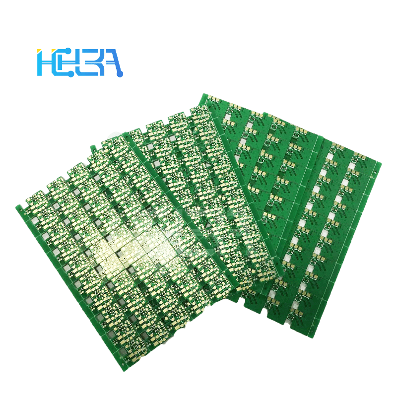
Hcjmpcba Keepout Aera In Pcb
Below are seven fundamental motivations (and advantages) for including keepout regions in PCB design. Some are obvious to experienced engineers; others are more subtle but equally critical.
A very common reason to use keepouts is mechanical integration: parts, enclosures, screws, standoffs, insertion clearances, connectors, and mating hardware often impose exclusion zones. Without keepouts, copper or components might collide with enclosure walls, screws, housings, shielding cans, or other mechanical elements.
Examples:
(1)A connector housing projects beyond the PCB plane; underneath or around that connector, you may need a keepout so no copper or via exists in that interference volume.
(2)Heatsinks, clips, or shielding cans might require spacing from copper or components.
(3)Movable parts (sliders, switches) may have motion paths that cross above the board; you might define a Z-axis keepout (i.e. vertical exclusion) to prevent any feature that intrudes beyond a certain height.
Hence, mechanical engineers and layout engineers must collaborate. The keepout serves as the “contractual” mechanical boundary enforced by the EDA tool, avoiding the risk that someone later places a trace under a screw or inside a screw clearance zone.
This is especially relevant in high-density PCB or multi-board systems, where subtle overhangs can produce reliability problems or enclosure collisions.
Keepouts also play a crucial role in preserving signal integrity and electromagnetic compatibility (EMC). In high-speed, high-frequency, or RF circuits:
(1)You may want to isolate sensitive signal traces or components from other copper to avoid coupling or noise injection.
(2)Around antenna areas (e.g. for wireless modules), you often place full-layer keepouts so no copper exists under or above the antenna region (i.e. no ground plane, no copper pour).
(3)For high-voltage circuits, creepage and clearance distances must be observed, and keepouts help enforce those distances physically.
(4)In analog sections near high-speed digital circuits, you may define keepouts to maintain guard rings or separation buffers.
Thus, a keepout enforces electrical isolation beyond what generic clearance rules might catch. It acts as a local exclusion that protects performance, reduces crosstalk, or prevents field interference.
Thermal and reliability concerns constitute another major reason for keepouts:
(1)In power-dense circuits, you may want to avoid copper around heat-dissipating components (e.g. power MOSFETs, linear regulators) to reduce thermal coupling or local hotspots.
(2)You may want to leave nonconductive clearance around temperature-sensitive parts (e.g. sensors) to reduce heat conduction or gradient stress.
(3)Around mounting holes or edges, solder fillets must maintain mechanical robustness; keepouts help avoid copper under holes or near edges where stress concentration or micro-cracking might occur.
Proper keepout planning can thus reduce warping, mechanical stress, and enhance long-term reliability under thermal cycling.
From an assembly / manufacturing standpoint, keepouts are critical to ensure:
(1)Access for pick-and-place heads, reflow ovens, wave solder, or probe stations. Components or traces must not block tool paths.
(2)Test fixtures, alignment pins, pogo pins, and probes must access their pads unobstructed.
(3)During rework or debugging, you need physical clearance to probe, solder, or de-solder components — keepouts prevent copper or vias under test fixture pads or clamping points.
Without keepouts, you might find that test probes short to underlying copper or you lose margin for soldering between a component pad and nearby copper. Proper keepouts safeguard practical assembly and test viability.
One of the often overlooked but crucial benefits of keepouts is communication and enforcement:
(1)A keepout region is visible to all designers, layout engineers, and DRC rules. It encodes constraints explicitly rather than relying on textual notes or PDF annotations (which are easy to ignore or misinterpret).
(2)It ensures that even if someone later re-routes or revisits the board, the exclusion remains enforced. It prevents “creep” of design rules.
(3)In a multi-discipline environment (mechanical, thermal, signal, compliance), the keepout is the boundary on which all teams align.
(4)Because it’s checked by the EDA tool, rule violations are caught early rather than slipping into fabrication.
Thus, a keepout is a durable “contract” between teams, reducing miscommunication errors and late-stage design corrections.
A very practical use case is to restrain how copper pours or via stitching fill the board:
(1)Suppose you have a large power plane or internal ground polygon. Without keepouts, copper might pour underneath an antenna or near mounting holes, violating your RF or mechanical goals.
(2)You may want to restrict via stitching or copper pour under certain areas — e.g. around sensitive analog circuits or shielding boundaries. A keepout on internal layers or “all-layer keepout” can block pouring or stitching there.
(3)Many designers wonder: Do Altium keepout layers also prevent planes from pouring? The answer is: yes — if you set the keepout region on the standard Keep-Out layer (not just a mechanical layer), it can block pours, stitching, tracks, etc.
(4)You can also combine keepouts with polygon cutouts or pour cutouts for fine control.
Therefore, keepouts give you granular control over copper fill behavior, overriding generic zone rules when necessary.
Finally, many keepouts relate to the board edge, mounting holes, slots, or cutouts:
(1)You typically don’t want copper to be too close to the edge — for mechanical robustness, insulation, or plating margin. A keepout zone ensures that copper, components, or vias maintain safe border clearance.
(2)Around slots, cutouts, or notches, keepouts help ensure that copper does not intrude into mechanical features or cause over-etching or breakouts.
(3)Some designers want to auto-generate keepouts from the board outline. In Altium, you can Design → Board Shape → Create Primitives From Board Shape, then convert those primitives to keepouts. Electrical Engineering Stack Exchange
(4)In practice, keepouts near edges or holes help avoid DFM issues, milling tolerance conflicts, or potential border copper peeling or delamination.
Because board shape is often communicated via mechanical layer or outline, keepout regions reinforce the buffer between copper / component space and the outline.
A keepout is only useful if you know how to define and enforce it in your EDA tool. Below we cover common workflows in Altium, KiCad, and general best practices.
Altium has robust support for keepouts (sometimes called “Region Keepouts” or “Object-Specific Keepouts”). Here’s a detailed view:
(1)In PCB Editor, you can place keepout primitives via Place → Keepout → Track, Region, Fill, Arc etc.
(2)Or use Object Specific Keepouts, which allow you to place a keepout attached to specific primitives.
(3)To generate a keepout following the board outline, you can use Design → Board Shape → Create Primitives From Board Shape, then convert those primitives to keepouts.
(4)For more complex keepout shapes, Altium supports Boolean operations (union, subtract) and region editing.
(1)A keepout can be specified as all-layer (placing it on the special Keep-Out layer) or layer-specific (only blocking e.g. top copper, internal layers, or bottom).
(2)If you choose the Keep-Out layer (the built-in special layer), the keepout will affect all layers by default (parts, tracks, vias, fills).
(3)If you place a keepout primitive only on a copper layer (e.g. “Top Layer”), it restricts only that copper layer’s features, not others.
(4)You can adjust properties in the region keepout object properties dialog (line style, cutout modes, layer scope) for finer control.
(1)A keepout region blocks polygon pours (or copper pour) from filling into its area, essentially acting as a cutout in the pour.
(2)However, note: in some older workflows or default settings, plane pours or internal plane layers might not always be fully blocked by keepouts unless you use the standard Keep-Out layer. Some users report that applying the keepout primitive only to top layer does not stop internal plane pours.
(3)If you encounter that your keepout is not blocking a plane, ensure the keepout is indeed defined on the Keep-Out layer (not a mechanical or copper layer) and that your clearance / pour rules allow respect of keepouts.
(1)Use a consistent mechanical or keepout layer naming convention (e.g., “Keepout”, “K_Out”) across projects to avoid confusion.
(2)Lock critical keepouts so they cannot be moved inadvertently.
(3)Use Boolean combine/subtract operations to manage overlapping exclusion zones.
(4)Use rule-based clearance enforcement in addition to keepouts — i.e. keepouts for special exceptions, general clearance rules for the rest.
(5)In collaborative multi-discipline workflows, mechanical/thermal/RF teams should review keepout zones before layout starts.
(6)For complex shapes (curved or organic outlines), approximate with many small segments or use imported DXF shapes converted to keepout.
(7)Before releasing to manufacturing, run a full DRC check to ensure no copper, via, or pad violates any keepout region.
KiCad’s approach to keepouts is evolving; the mechanism is slightly different from Altium and has both strengths and limitations.
(1)In KiCad PCB Editor (Pcbnew), you can define rule areas (keepout zones) which can disable tracks, vias, pads, footprints, or copper fills in that region.
(2)Use the Add Keepout Zone tool (icon in side toolbar) and in the dialog specify which features are disallowed (tracks, vias, copper fills, footprints).
(3)For footprint-level keepouts (e.g. a component demands a local exclusion region), the KLC (KiCad Library Convention) suggests drawing a “rule-area (keepout)” and naming it (e.g. “Antenna Keepout”).
(4)In some tool versions, the dialog lets you choose which layers the keepout applies to. In KiCad 8+, the rule-area creation dialog includes layer selection (though not all user layers are supported).
(1)Creating a perfect circular keepout is not always directly supported. Many users approximate circle shapes by polygonal segmentation.
(2)For mounting holes, designers often combine clearance settings on the hole pad with a keepout zone around it.
(3)The circle drawing tool on Edge.Cuts layer in KiCad can define board outline; interestingly, the area inside the circle can act as a keepout by virtue of how KiCad treats internal vs external areas.
(4)Some community discussions note limitations or bugs: e.g. resizing keepout definitions in footprint editor, or inability to place rule-area on certain layers.
(1)In some older KiCad versions (5.x), footprint-level keepouts were limited; many designers resorted to using graphical layers with names like “keepout,” but those won’t be enforced by DRC.
(2)Custom DRC rules can be used to allow or disallow exceptions inside keepout areas (e.g. allow certain nets or tracks) — though it’s more manual.
(3)Sometimes keepouts do not automatically block copper fill in zones if they are placed after filling; you may need to re-fill or re-run the zone with cutouts.
(4)KiCad community has open feature requests to enhance keepout behavior (e.g. allowing silkscreen / copper fill keepouts more flexibly)
Overall, KiCad’s keepout mechanism is serviceable, especially in newer versions, but you should validate with DRC and be cautious about tool limitations.
Below are cross-tool guidelines and best-practice strategies:
3.3.1 Margin strategy
Define keepout clearances generous enough to absorb tolerances (e.g. mechanical misalignment, drill registration error).
Don’t over-constrain: overly aggressive keepouts can force routing detours, increase track length, or complicate layout.
3.3.2 Layer scoping
Use all-layer keepouts only where needed (e.g. around antennas, mechanical holes).
For less critical regions, restrict to certain copper layers to maintain routing flexibility.
3.3.3 Version control & locking
Lock critical keepout primitives so that they aren’t moved by layout tweaks.
Use version control (Git, SVN) so you can track changes to keepout definitions.
3.3.4 DRC & design reviews
Always combine keepout enforcement with general clearance rules; use DRC to catch any violations.
Include keepout review in your peer review / DFT / DFM checklists.
3.3.5 Collaboration between disciplines
Engage mechanical, thermal, RF, and compliance teams early to define keepouts before layout.
Ensure that keepout definitions are documented (in design docs or mechanical drawings) and communicated clearly.
3.3.6 Balancing flexibility and rigidity
Don’t use keepouts as a substitute for routing rule planning; instead, use them as meaningful exceptions or constraints for critical zones.
Be cautious of overlapping or conflicting keepouts; use Boolean logic or region subtraction to manage them.
3.3.7 Test & validation
After placement of keepouts, run DRC, generate Gerber preview, and do visual inspection to ensure no copper or pad leakage.
For prototypes, validate mechanical clearance with 3D models or tolerance stacking.
By combining good keepout strategy with robust rules and review, designers can avoid many late-stage surprises.
Hcjmpcba On The Keepout
Q: Do I need a keepout for a connector?
A: Usually yes — connectors often impose overhang, mechanical tolerances, mating or insertion clearance, or board-edge proximity constraints. By placing a keepout around the connector region (or underneath connector footprints), you prevent copper traces or vias interfering with mechanical clearance. This is especially important for right-angle connectors or connectors with metal shielding tabs.
Q: Does 960 have keepout zones?
Here “960” might refer to a particular layout standard, board size, or internal project code. Strictly speaking, “960” does not inherently define keepout zones — keepouts are defined by the designer based on mechanical, electrical, or manufacturing constraints. If in your internal standard “960” means a board dimension or class, then you may have default keepouts around borders or mounting holes, but these are not universal.
However, if your question is “Does IPC-960” or a standard named “960” include keepout definitions?, as of knowledge cutoff, no standard “960” is widely known that mandates keepout zones; designers must define keepouts based on their application needs.
Q: Do Altium keepout layers also prevent planes from pouring?
Yes — when the keepout primitive is placed on the standard Keep-Out layer, it can block plane or polygon pours across all copper layers, preventing copper or void fill inside the keepout.
Be careful: if you place the keepout only on a mechanical or copper layer rather than the special Keep-Out layer, you may not block internal plane pours. Hence use the built-in keepout layer for full effect.
Q: Does a “keep out keep out” or “keepout sign” query have special meaning?
These are likely user search artifacts (e.g. repeated words). In terms of PCB design, “keepout sign” might refer to labeling or markings on the board (silkscreen) indicating keepout area. But technically, the functional enforcement is via the keepout primitive in the layout; the sign (silkscreen) is secondary for human readability.
Q: Should I always use keepout around mounting holes / test pads?
Yes — as a safe default, it is prudent to impose keepouts around mounting holes, test pads, or fiducials. These are high-risk zones where mechanical stress, probe contact, or tooling may interact with underlying copper. The keepout ensures no copper or traces will lie directly underneath or too near. But the clearance size can vary — simple boards might leave minimal clearance, while high-reliability designs use generous buffer zones.
Q: What about “outlayer” or “altium keepout layer board outline”?
“Outlayer” is a less common synonym for an exclusion layer or mechanical layer tied to keepout concept. In Altium, using board outline primitives converted to keepouts bridges board shape and keepout definition: you can make a keepout around the board perimeter by converting outline tracks to keepout objects. This is especially useful when you want enforcement directly tied to the board outline.
Q: What about kicad circular keepout?
Because KiCad doesn’t always let you draw perfect circles for keepout zones, designers often approximate circular keepouts using segmented polygons. For mounting holes or circular sensor regions, combine hole clearance and a polygonal keepout ring.
If KiCad version supports rule-area with layer selection, you may place circular rule areas (approximated) to enforce exclusion. In newer versions (KiCad 8+), you can choose which layers the area applies to.
Q: What if my keepout is violated in fab / review?
If DRC or manufacturability review flags a keepout invalidation (copper or via inside keepout region), you should:
Evaluate whether the keepout or object is wrongly defined (layer scope, region assignment, locking).
Check if clearance or rule settings override the keepout (rare, but possible).
Move or reroute the offending object.
If absolutely necessary and justified, relax or shrink the keepout — but that should only happen after cross-discipline agreement, not last-minute fixes.
Here are the major points to remember, as a reference for both engineers and decision-makers:
5.1 A keepout is a software-enforced exclusion region that disallows copper, vias, or components; it’s more robust than notes or annotations.
5.2The seven primary reasons to use keepouts are:
(1)Mechanical / enclosure constraints
(2)Electrical / signal integrity / EMI isolation
(3)Thermal / reliability buffer
(4)Manufacturability / assembly / test access
(5)Communication & rule enforcement
(6)Copper pour & via stitching control
(7)Edge clearance & board outline constraints
5.3 In Altium, use either object-specific keepouts or the special Keep-Out layer for all-layer exclusion; convert board outline to keepouts if desired.
5.4 In KiCad, use rule-area (keepout zones) and specify which features to disallow; approximate circular shapes when needed, and check tool limitations.
5.5 Best practices include judicious margin sizing, locking keepout primitives, combining with DRC, cross-disciplinary review, and avoiding over-constraint.
5.6 Common pitfalls include forgetting to scope keepouts to all layers, relying only on textual notes, or late-stage changes that violate exclusion zones.
Therefore, when you receive a design file or check with a prospective buyer, confirm that keepout zones are properly defined, understood, and enforceable in the chosen tool and fabrication flow.
Discover the 7 powerful strategies to evaluate and select the best Automotive PCB Fabrication & Asse

This article focuses on "what is pcb assembly", systematically introduces the classification, compon
Guangzhou Huachuang Precision Technology Co., Ltd. (HCJMPCBA) specializes in ISO 13485-certified Bl


