Huachuang PCBA Processing Factory: High – speed Chip Mounters – The Core Driving Force of Electronic Manufacturing
This article focuses on the high - speed chip mounters in Huachuang PCBA Processing Factory. It firs
A Ball Grid Array (BGA) is an advanced semiconductor package that uses an array of solder balls (metal balls) for electrical and mechanical connection to a PCB. Quality control of BGA components requires controlled reflow soldering, X-ray inspection, and full traceability. This guide is maintained by the HCJMPCBA engineering team and updated with production checklists.
BGA packages enable high-density, high-performance electronics but require strict process control
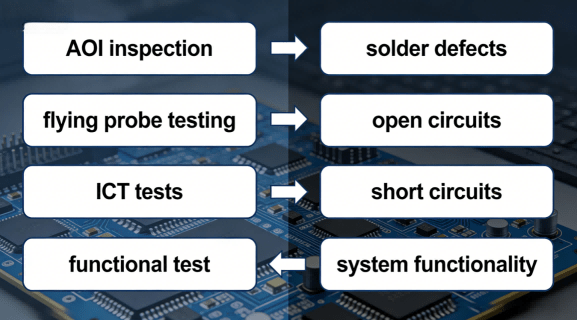
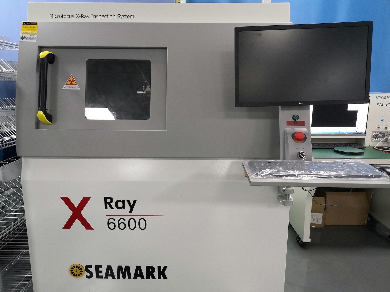
Invisible solder joints demand X-ray-based inspection and data validation
HCJMPCBA ensures reliability through Method-controlled processes, traceability, and raw data transparency
A Ball Grid Array (BGA), also referred to as a bga package, is a surface-mount packaging technology where electrical connections are made through an array of solder balls (metal balls) located beneath the component.
Unlike traditional leaded packages, BGA components use:
shorter electrical paths
improved thermal dissipation
higher pin density
This is why modern bga processors, bga chips, and high-speed devices rely on this structure.
PBGA (Plastic Ball Grid Array)
CBGA (Ceramic BGA)
FBGA (Fine-pitch BGA)
TBGA (Tape BGA)
Each bga type package differs in thermal expansion, reliability, and application environment.
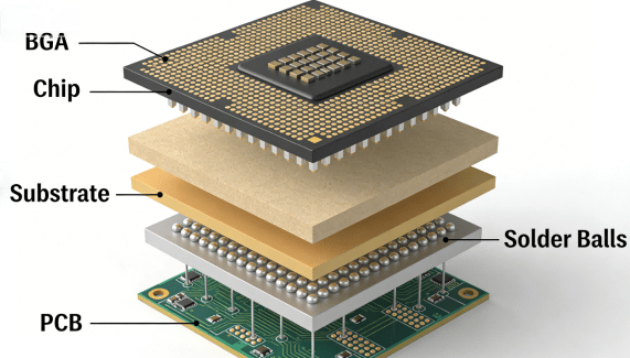
3d Sectional View Of Bga Ball Structure
Ball grid array soldering is a reflow-based process where solder balls melt and form metallurgical bonds between the bga chip and PCB pads.
Flux activation removes oxides
Solder balls melt at controlled temperature
Surface tension aligns components
According to IPC J-STD-001, proper thermal profiling is essential.
Precision stencil printing ensures correct volume deposition
High-accuracy pick-and-place aligns the bga components
Controlled thermal profile forms reliable joints
Detects voids, bridging, and missing balls
Validates electrical performance
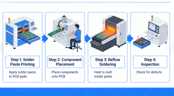
Smt + Reflow Soldering Process
At HCJMPCBA, BGA quality is managed through a structured system:
Method No.: HCJM-BGA-2026 Rev.3
Defines:
soldering parameters
inspection criteria
acceptance thresholds
Based on ANSI/ASQ Z1.4
AQL-based sampling
batch-level inspection
thermal cycling (-40°C to +125°C)
mechanical stress simulation
electrical continuity testing
Clients receive:
X-ray images
inspection reports
process logs
Each bga circuit board is traceable to:
solder paste batch
component lot
production time

Comparison Between Good Products Vs. Voidsbridging Defects
| Defect Type | Cause | Risk Level | Action |
|---|---|---|---|
| Voiding | trapped flux | medium | optimize profile |
| Bridging | excess solder | high | adjust stencil |
| Head-in-pillow | poor wetting | high | improve flux |
| Missing ball | placement issue | critical | reject |
| Test | Method | Standard |
|---|---|---|
| X-Ray Inspection | IPC-7095 | void <25% |
| Thermal Cycling | IEC standard | no crack |
| Functional Test | custom | pass rate 100% |
1.Using generic reflow profiles
2.Ignoring moisture sensitivity of BGA components
3.No X-ray inspection
4.Poor stencil design
5.Lack of traceability system
Ball grid array rework must be carefully controlled:
localized heating
controlled cooling
reballing if required
Improper rework can damage the bga pcb permanently.
Ball grid array rework must be carefully controlled:
localized heating
controlled cooling
reballing if required
Improper rework can damage the bga pcb permanently.
Hcjm Pcba Pcb Manufacturing & Assembly Supplier Services 1
Supplier must provide:
BGA X-ray inspection reports for each batch
Full traceability (lot/batch/serial)
Defined process method (Method No. + Revision)
Thermal profile documentation
Raw X-ray images
Thermal profile logs
AOI/X-ray reports
Material certificates
Raw X-ray images
Thermal profile logs
AOI/X-ray reports
Material certificates
Q:What is a BGA in electronics?
A:A BGA (Ball Grid Array) is a semiconductor package using solder balls for PCB connection.
Q:Why are BGA packages better?
A:They offer better heat dissipation and higher density than traditional packages.
Q:What is BGA testing?
A:It includes X-ray inspection, thermal cycling, and electrical validation.
Q:Can BGA be repaired?
A:Yes, but ball grid array rework requires specialized equipment.
Q:What causes BGA failure?
A:Thermal stress, poor soldering, or void formation.
Understanding what is a ball grid array is only the first step. Ensuring reliability requires:
controlled processes
inspection systems
traceability
HCJMPCBA positions itself not just as a manufacturer, but as a process authority in BGA electronics.
Update triggers: standard revision changes / recurring questions / production checklist updates.
This article focuses on the high - speed chip mounters in Huachuang PCBA Processing Factory. It firs
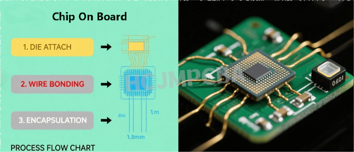
Chip on board (COB) is a sophisticated electronic packaging method where bare semiconductor dies are
Guangzhou Huachuang Precision Technology Co., Ltd. (HCJMPCBA) specializes in ISO 13485-certified Bl