10 Essential Things You Need to Know About SMD 0805: Can You Probe 0805 & More for PCBA Projects
Wondering “can you probe 0805” SMD components or need clarity on 0805 resistor size, power ratin
Wondering “can you probe 0805” SMD components or need clarity on 0805 resistor size, power ratin
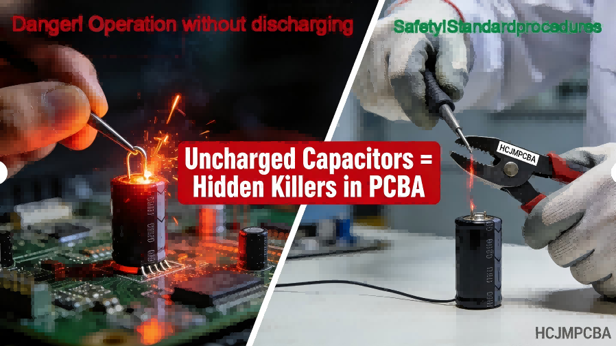
Discharging capacitors is a critical safety and quality control step in electronics and PCBA work. T
A circuit card assembly is a complete electronic unit created when components are mounted, soldered,


