HCJMPCBA | Precision BGA & PCB Assembly Solutions
Guangzhou Huachuang Precision Technology specializes in high-reliability BGA assembly, offering prec
Understanding what does most damage to circuit board is essential for maintaining reliable pcb circuits. From component failures to burnt traces and moisture-related corrosion, circuit board damage can jeopardize product durability and performance. This guide explores the most common causes of PCB damage, how to identify issues like burnt SMD resistor or burnt circuit board, how to perform circuit board repair or pcb board fix, and ways to prevent future board burns.
excessive current flow, thermal stress, or inadequate cooling often leads to a burnt circuit board or burnt PCB trace—a key factor in pcb circuits failure. Extreme heat may scorch components or warp layers, often initiated by poor ventilation or overloaded traces.
Techniques to mitigate this include proper venting, using thermal vias, and maintaining generous clearance around heat-generating parts.
When current travels along unintended paths—due to solder bridges, contamination, or design flaws—it can produce arcs or burnouts. Such what does most damage to circuit board scenarios often involve arcing between power planes, leading to massive trace erosion.Minimizing this requires adequate creepage distances and robust insulation.
Exposed to humidity or dust, pcb circuits suffer from conductive corrosion and degraded dielectric properties—leading to shorts or intermittent faults. Aging components can overheat as efficiency drops. These environmental stressors quietly damage boards over time.
Issues like poor trace width, copper-to-edge clearance problems, acid traps, or cold solder joints often create pcb circuits vulnerabilities. These can lead to burn board failures or trace fatigue.
Temperature cycles and vibration drive solder fatigue, resulting in cracked joints. This higher resistance can induce hot spots, leading to board burn or faulty circuit board behavior.
Flexing, testing, or connector insertion can cause pad cratering, literally fracturing the pad and underlying fiberglass—compromising solder integrity and electrical continuity.
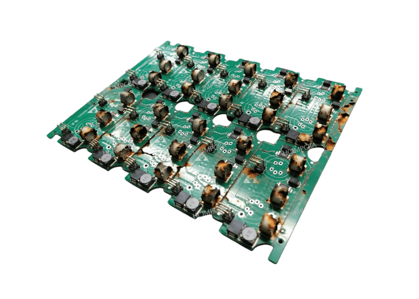
Signs include charred traces, blackened components, warped areas, blown conformal coating, or delaminated regions. A burn PCB looks visibly scorched or cracked.
Use thermal imaging, insulation-resistance testing, or probe measurements to locate faulty circuit board areas, shorts, or open paths.
Intermittent malfunctions, overcurrent trips, or complete device shutdowns signal serious internal issues—often due to burning circuit boards or component failure.
Power down and inspect visually; clear dust and contaminants. Identify burnt SMD resistor or charred areas. Use a heat gun or soldering tools cautiously to access damaged areas.
Patch a burnt PCB trace using copper foil tape, jumper wires, or trace repair kits. After restoring continuity, apply epoxy or conformal coating to protect the fix.
Remove damaged components and solder new ones using precision rework gear. Ensure proper alignment, use of ic board repair techniques, and inspect for pcb repair viability.
If pad cratering, extensive delamination, or multi-layer damage occurs, full board replacement may be safer and more reliable.
Ensure good airflow, add fans or thermal vias, avoid overworking high-power components, and use components rated for expected temperatures.
Keep boards clean and dry, avoid exposure to sunlight or moisture, and seal enclosures in harsh conditions.
Maintain adequate trace spacing, appropriate copper weight, and avoid thermal stress points (like acid traps). Employ DFM checks to enforce design quality.
Use certified parts, follow soldering best practices, and mitigate ESD and solder defects that contribute to long-term pcb circuits degradation.
Design in fuses, thermal cutoffs, and monitoring circuits to prevent overload-induced failures.
| Damage Cause | Impact on PCB Circuits | Prevention Strategy |
|---|---|---|
| Overheating / Thermal Burn | Burnt traces/components | Optimize cooling, layout, thermal design |
| Short Circuits / Arc Damage | Trace erosion, ignitions | Adequate spacing, insulation |
| Moisture / Aging | Corrosion, shorts, degraded performance | Enclosure sealing, humidity control |
| Manufacturing Flaws | Cracked traces, faulty joints | DFM, soldering standards, design review |
| Solder Fatigue / Mechanical Stress | Cracked joints, intermittent connection | Material selection, thermal cycle design |
Guangzhou Huachuang Precision Technology specializes in high-reliability BGA assembly, offering prec

Learn exactly how to convert watts to amps in DC, single-phase AC, and three-phase systems with clea
PCB warpage is a critical issue in medical devices, AI hardware, and industrial automation, where di


