Understanding what a PCB (Printed Circuit Board) stands for isn’t just academic—it’s fundamental for OEM engineers, buyers, and end-users in today’s electronics market. HCJMPCBA explores that definition in depth, and reveals how advanced tools like an ict tester ensure quality and reliability in PCB assembly.
1. What Does PCB Stand For—and What About PCBA?
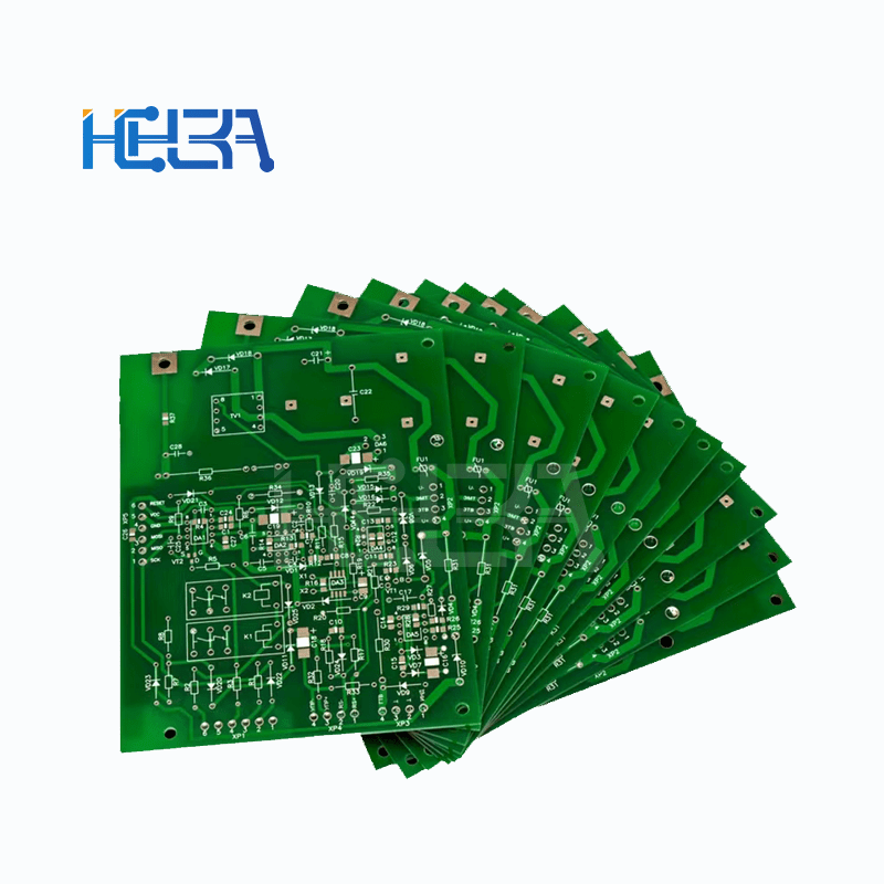
PCB stands for Printed Circuit Board, a foundational element in electronic devices. It’s a rigid or flexible board that provides mechanical support and electrical connections via etched copper traces, insulating substrates, solder masks, and silkscreen labels.
PCBA, or Printed Circuit Board Assembly, refers to a PCB populated with electronic components, making a complete circuit card assembly. This distinction is essential when sourcing electronics manufacturing partners.
2. What Are Circuit Boards Made Of? Key Materials & Processes
Typical PCBs use fiberglass epoxy (FR-4) or flexible substrates with copper layers etched into traces. These are insulated with solder mask and annotated via silkscreen printing.
Modern demands compel adherence to lead free soldering standards for health and compliance, particularly under RoHS regulations. Appropriate materials and finishes, like ENIG or OSP, support long-term durability.
3. Key Assembly Concepts: SMD, Keyboard PCBs & Cold Joints
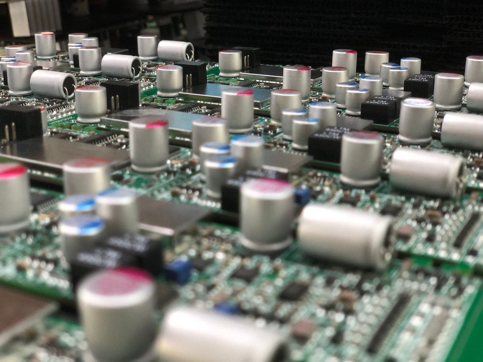
SMD (Surface Mount Device) technology enables high-density mounting on PCBs, pivotal in industrial pcb production. Components are placed via automated pick-and-place machines, improving speed and compactness.
A keyboard PCB often illustrates complex, multi-layer board assemblies with mixed SMD and through-hole components—ideal for highlighting PCBA flexibility.
Cold joint soldering refers to a poor solder connection caused by inadequate heat or movement during cooling, leading to weak conductivity or failure—a known issue in the soldering process.
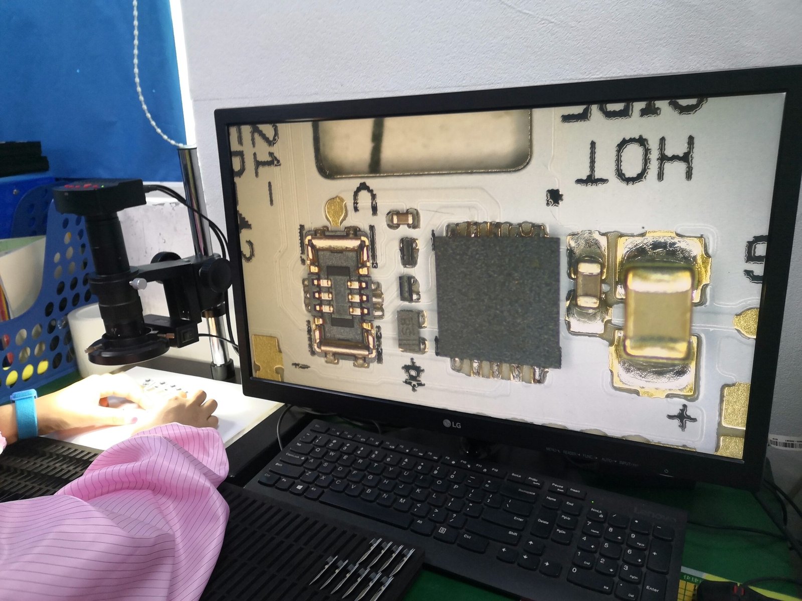
4. Safeguarding Quality with an ICT Tester
An ict tester (In-Circuit Tester) uses probe-based testing—commonly with a bed-of-nails fixture or flying probe—to evaluate individual components on PCBAs. This ensures correct placement, polarity, and functionality at scale.
1.Bed-of-nails setups are ideal for high-volume runs.
2.Flying probe systems offer flexibility for prototypes or low-volume batches.
HCJMPCBA incorporates ICT testing to verify layout accuracy and reliability before proceeding to final steps.
5. From Gerber File to Full PCBA Workflow
Key steps in industrial pcb production include:
1.PCB Design & Gerber file output
2.PCB fabrication using copper layering, etching, drilling
3.Component placement and lead free soldering
4.ICT testing for quality validation
5.Final inspection (AOI, functional tests) and packaging
Using this process, HCJMPCBA delivers reliable circuit card assemblies that meet both performance and compliance standards.
6. Why This Knowledge Equips Procurement Teams
Understanding terms like pcba meaning, gerber file, and ict tester designates professionalism in vendor communication. It ensures better supplier selection, negotiations, and quality expectations—especially when partnering with providers like HCJMPCBA.
7. FAQ
1.What does PCB stand for? Printed Circuit Board.
2.Why is PCBA different from PCB? PCBA adds the electronic components to a PCB.
3.What role does an ICT tester play? Validates component-level connectivity and performance.
4.What materials make up PCB boards? FR-4 or flexible substrate with copper, solder mask, and silkscreen.
Grasping what PCB means—and the associated manufacturing steps like ic tester quality checks, lead free soldering, or gerber file generation—enhances sourcing intelligence and success. HCJMPCBA combines term clarity with top-tier execution.