
Understanding PCB Attenuation: Why Signal Loss Matters & How HCJMPCBA Ensures Integrity
Discover what attenuation means in PCB signal transmission—why signal loss matters, what causes it
In today’s electronics manufacturing world, a well-constructed circuit diagram is far more than a drawing — it is the logical blueprint of a system, the foundation for every successful PCB/PCBA project. From high-speed telecom modules to automotive ECUs, engineers and procurement decision-makers rely on accurate pcb schematic documents to ensure functionality, manufacturability, and quality. Understanding how to read and interpret these diagrams elevates the entire process of sourcing, assembling, and delivering printed circuit board assemblies.
A circuit diagram is a graphical representation of an electrical circuit, showing how components are connected via standardized symbols and lines.It serves multiple purposes: clarifying function, guiding layout, supporting test/repair.
In the context of printed circuit boards, this diagram is often referred to as a pcb schematic, circuit board schematic, or schematic diagram of pcb — terms your OEM engineering or procurement team may search when verifying documentation or working with a PCBA supplier.
It’s important to distinguish these related terms:
Circuit diagram (general): shows component connections, may be technology-agnostic.
PCB schematic: specifically a diagram for PCB design, showing nets, components, nodes and their relationships.
PCB layout (or board layout): the next step, physically placing components and routing traces — often derived from the schematic.
Thus: schematic → netlist → layout. Your sourcing team may request the schematic to evaluate how well the design is documented, and whether it aligns with what you plan to manufacture.
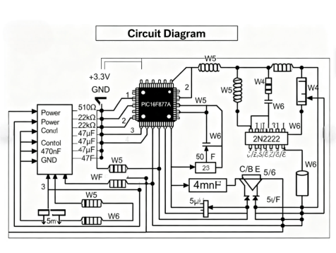
Hcjmpcba A Circuit Schematic Diagram Of Actual Electrical Connections
In a quality circuit diagram, symbols convey meaning instantly:
Resistors (R), capacitors (C), inductors (L)
Diodes (D), transistors (Q), integrated circuits (U/IC)
Connectors (J/CON), power supply (PS), switches (SW)
Knowing these allows you to read circuit schematics quickly and verify correct components.
Nets: Conductive paths connecting component pins (e.g., “VCC”, “GND”, “DATA_IN”)
Nodes: Points in a circuit where multiple nets converge
Reference designators: Unique labels (R1, C5, U3) to identify each instance
When you receive a pcb board circuit diagram, checking for clear nets and designators is key to reliability and traceability.
Begin by locating the main rails: VCC, GND. Then follow primary signal paths. In a complex pcb schematic, this first step gives context.
Most schematics are arranged logically: inputs on the left, outputs on the right, power rails on top/bottom. This flow aids readability.
Large assemblies use multiple sheets. Look for “Page A → Page B” connectors. When reviewing a pcb circuit diagram, ensure cross references and continuity.
If you see a symbol for a resistor network or unclear wiring, use the schematic to verify placement and interpretation. A well-drafted diagram simplifies troubleshooting and even maintenance.
Modern ECAD tools export schematics in formats like .SCH, .PDF, or .SVG, and generate netlists (.NET). These become input for layout tools.
Adhering to standards such as IEC 60617 or ANSI/Y32.2 ensures clarity across regions.
Pro tip: Use consistent page naming (A_Block, B_Power) and keep comments/revision history in the title block.
Once your diagram is complete, the layout team uses the netlist to place components and route traces in the pcb manufacturing process. A clean schematic shortens DFM review and reduces errors.
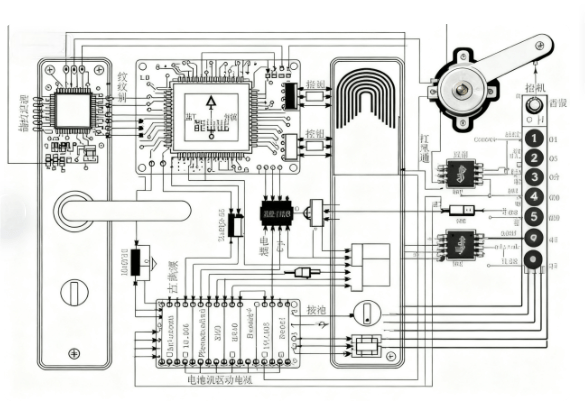
Hcjmpcba Electrical Pcb Schematic Diagram Of A Doorbell Circuit
Dense wiring without labels makes reviews difficult and increases risk of board rework.
Breaking numbering rules (e.g., repeating R1 twice) causes confusion during BOM/assembly.
When procurement requests a “pcb board circuit diagram,” missing document links slow down quoting and production.
Use standardized symbols and nets
Include revision history and page directory
Ensure schematic mirrors board reality
Validate netlists and BOM before issuing to manufacturer
A precise circuit diagram bridges conceptual design and manufacturing. The manufacturer (like HCJMPCBA) can interpret the schematic, produce the PCB, and assemble with confidence.
Poor schematics increase risk of mis-placed components, wrong nets, and failed boards. A proper schematic saves rework and scrap.
For high-reliability sectors, a schematic becomes part of your quality system. Clear documentation supports traceability, change control, and compliance.
At HCJMPCBA, we receive your schematic, perform DFM/DFT review, then generate the PCB layout and assembly lines. This seamless workflow minimizes translation errors.
For a European automotive ECU project, we used the customer’s multi-sheet schematic, conducted netlist verification, generated Gerbers, and delivered 100 k units with <0.3% defect rate.
We provide a “schematic review checklist,” offer feedback on net labeling and revision tracking, and help you convert your diagram circuits into manufacturing-ready files.
Q: What is the difference between a circuit diagram and a schematic?
A: A circuit diagram is a general term showing connections; a schematic (especially a pcb schematic) uses standardized symbols and is often the input for board manufacturing.
Q: How many pages does a typical PCB schematic have?
A: It depends on complexity — consumer boards may fit one sheet; high-density industrial boards may have 5-10 sheets or more, with cross-references.
Q: What file types are used for electronic circuit diagrams?
A: Common formats include .SCH, .PDF for schematics, and netlists (.NET), Gerber (.GBR) for layout.
Q: Can I convert a circuit diagram to manufacturing files myself?
A: In principle yes, but you need EDA tools, accurate BOM, and layout rules. Many OEMs prefer to work with a trusted supplier like HCJMPCBA to avoid mistakes.
Q: How to read resistors and other components in a schematic?
A: Components have reference designators (e.g., R1, C2). Nets and nodes show connections. Learning symbols and flow is key to reading a schematic.
In summary, a well-crafted circuit diagram is the cornerstone of a smooth, high-quality PCBA manufacturing process. From understanding nets and symbols, to designing a clean pcb schematic, to partnering with a reliable manufacturer, each step matters. When you choose HCJMPCBA, you’re selecting a partner that values precision, clarity, and seamless transitions from diagram to production.
Learn more about PCBA services, please contact Guangzhou Huachuang Precision Technology.
Discover what attenuation means in PCB signal transmission—why signal loss matters, what causes it

Guangzhou Huachuang Precision Technology Co., Ltd. offers fast, high-quality PCBA solutions with a f
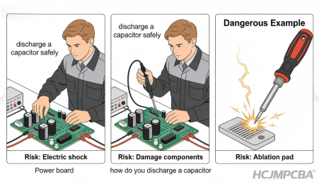
Need to know how to discharge a capacitor safely before troubleshooting, PCB repair, or disassembly?


