5 Safe and Effective Methods: How to Clean Battery Corrosion in Remote and Other Electronics
Learn how to clean battery corrosion in remote control devices and other electronics with safe, step
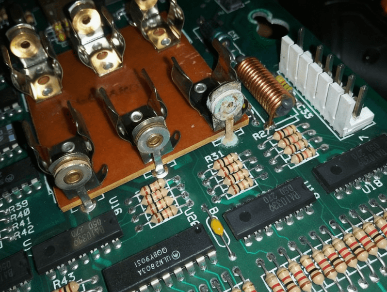
A PCB — short for Printed Circuit Board — is the foundational backbone of virtually all electronic devices. It is a flat board typically built on a non-conductive substrate (such as fiberglass) with conductive copper traces etched or laminated onto or between layers. These traces serve as the “wiring system,” enabling electronic components (like resistors, capacitors, ICs) to be mounted on pads and connected in a reliable, repeatable pattern.
In practical manufacturing workflows, a bare PCB (“blank board”) becomes a fully functional circuit module when populated with components — a process commonly referred to as PCBA (PCB Assembly). At HCJMPCBA, we combine PCB fabrication, component procurement, SMT/THT assembly and testing — delivering turnkey PCBA solutions for our clients.
Why does PCB matter? Because it enables miniaturization, reliability, scalability, and cost-effective mass production. A well-designed PCB ensures that devices — from consumer electronics and medical gadgets to industrial controllers and power systems — are compact, durable, and manufacturable at scale.
As a high-tech enterprise with decades of experience in PCB R&D, manufacturing and certified PCBA assembly, HCJMPCBA understands that the quality of the PCB (materials, layout, manufacturing) directly affects the end product’s performance, reliability, and manufacturability.
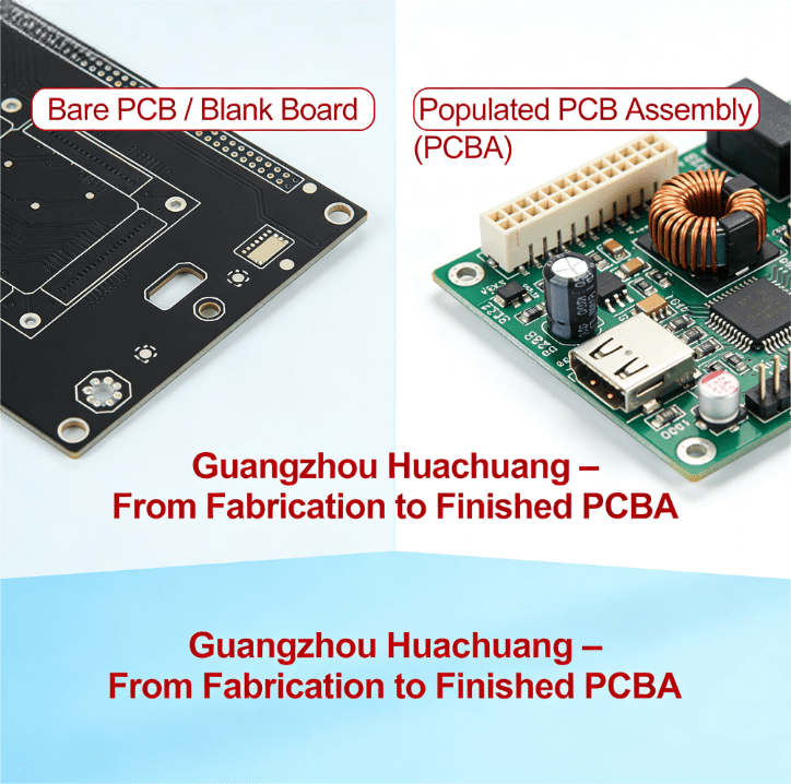
Hcjmpcba Comparison Between Pcb Bare Boards And Pcba With Components Installed
A typical PCB consists of several material layers, each serving a specific function. The main elements include:
Substrate (Base Material): Usually a fiberglass-epoxy laminate (e.g. FR-4), which provides mechanical support and insulation. Some PCBs use specialized materials (metal core, flexible substrates) depending on thermal, mechanical or form-factor requirements.
Copper Layers: Thin copper foil laminated onto (or between) substrate layers. These are etched to form conductive traces, pads, and planes — the “wiring” of the circuit.
Solder Mask: A protective insulating layer applied over the copper traces (except pads) to prevent solder bridging, corrosion, and shorts during assembly.
Silkscreen (Legend): Printed markings on the board for component designators, logos, version info — essential for assembly, testing, maintenance, and repair.
Depending on product requirements, PCB materials can be tailored — standard FR-4 for general electronics, high-Tg or metal-core laminates for power or high-temperature applications, or flexible substrates for wearable / folded devices. HCJMPCBA supports custom substrate selection (rigid FR-4, metal-core, flexible, rigid-flex, etc.) to match thermal, mechanical, and space demands.
PCBs are commonly classified based on number of conductive layers and board structure.
Single-sided PCB: Single copper layer on one side — used for simple circuits and low-cost devices.
Double-sided PCB: Copper on both sides, with through-holes or vias for interconnection — supports more complex circuits and dual-side component placement.
Multilayer PCB: Multiple (e.g. 4, 6, 8… up to dozens) conductive layers bonded together with insulating prepreg layers. Enables high-density routing, compact design, and complex power / signal distribution — essential for high-performance, high-density electronics such as motherboards, communication devices, medical electronics, etc.
Rigid-Flex / Flex PCBs: Use flexible substrate (or combination of rigid + flex) — suitable for devices needing folding, bending, or space-constrained integration (e.g. wearable, portable, curved devices). Flexible PCBs are increasingly used where form factor, weight, or mechanical flexibility matters.
Understanding how a PCB is manufactured helps engineers, buyers, and decision-makers appreciate the value and complexity behind each board. It also highlights where quality and precision matter — exactly where a reliable supplier like HCJMPCBA makes a difference.
The fabrication process typically includes the following steps:
Design & Layout → Gerber / CAM Data generation: Engineers use PCB CAD tools to create schematics, footprint placement, trace routing, stack-up configuration. Final output uses standard manufacturing file formats (e.g. Gerber + drill data) for fabrication.
Photo-film / Mask Creation & Imaging: Gerber data is converted into photo films which define copper patterns for each layer. These films act as templates for etching.
Etching / Inner Layer Processing (for multilayer boards): Inner copper layers are etched to form their circuit patterns.
Layer Stacking & Lamination: For multilayer PCBs, inner layers, insulating prepreg and outer copper layers are stacked and laminated under heat and pressure — forming a solid, unified board. Precise alignment (within microns) is critical.
Drilling / Via Formation: Holes (through-holes / vias) are drilled to connect layers electrically. These are then plated to form conductive inter-layer connections.
Outer Layer Etching, Solder Mask & Silkscreen: Copper traces are etched, then solder mask is applied for insulation/protection, followed by silkscreen for part marking and identifiers. Surface finish (e.g. HASL, ENIG) may be applied depending on requirements.
Cutting / Profiling / Depanelization: The manufactured panels are cut or routed into individual PCBs, including any required board shaping, mounting holes, beveling.
Final Inspection & Quality Control: Visual inspection, dimensional checks, electrical testing (e.g. continuity / isolation tests) to ensure board meets design specs before shipping.
After fabrication, PCBs proceed to component mounting (assembly) — which is part of PCBA.
Once the bare PCB is ready, it’s populated with components per design (BOM) using SMT (Surface Mount Technology) or through-hole / mixed assembly. For high-density or fine-pitch PCBs, SMT with automated pick-and-place, reflow soldering, and quality inspection is standard.
After mounting and soldering, quality control steps (optical inspection, functional testing, possibly X-ray / ICT / FCT for complex or critical boards) ensure reliability and performance before delivery. HCJMPCBA provides full PCBA services: PCB fabrication → component sourcing → SMT / THT assembly → testing → delivery — a one-stop solution for OEM clients.
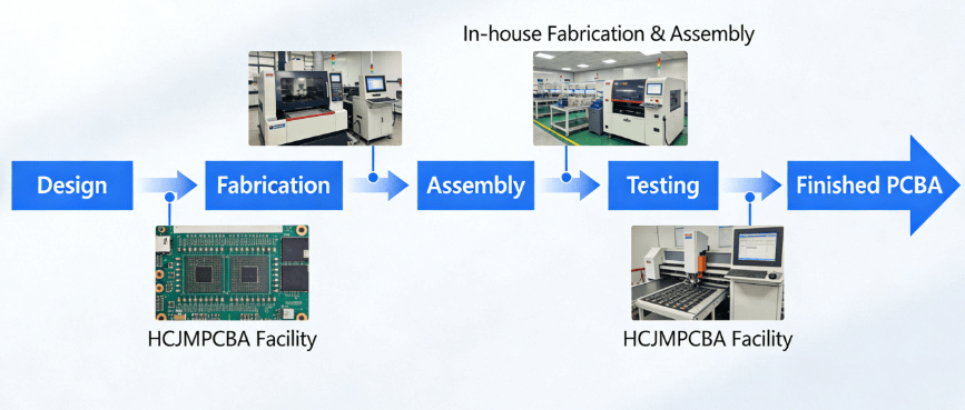
Hcjmpcba Pcb Manufacturing Process Flow Chart
Using PCBs instead of manual wiring or point-to-point wiring brings multiple advantages, especially relevant for engineers, buying managers and procurement decision-makers.
Compactness & Miniaturization: Multi-layer PCBs and surface-mount technology allow extremely dense circuit layouts — essential for modern electronics, wearable devices, medical instruments, IoT, etc.
Manufacturability & Scalability: Once a PCB design is verified, identical boards can be mass-produced reliably and cost-effectively. This scalability reduces per-unit cost for large runs and ensures consistency across units — a critical benefit for OEMs and buyers managing global supply chains.
Reliability & Consistency: Automated fabrication and assembly reduce human wiring errors. Solder mask, solder joints, rigid structure improve durability, mechanical stability, and electrical integrity over time.
Support for Complex Signals & High-Speed / High-Density Circuits: For advanced electronics requiring controlled impedance, multiple power/ground planes, high-speed data lines — multi-layer PCBs provide the electrical and structural foundation that simple wiring cannot.
Ease of Maintenance, Testing, Traceability & Modular Design: PCBs with silkscreened labels, standard footprints, test points, and layout standardization make assembly, troubleshooting, maintenance, and future revisions much easier — advantages for product lifecycle management and supply chain stability.
For procurement decision-makers, these advantages translate into lower total cost of ownership, predictable quality, reduced rework, scalable manufacturing, and supply-chain stability — which are critical for business success.
Not all PCBs are equal. Depending on product requirements (space, thermal management, mechanical durability, flexibility, cost), the right PCB type and material must be selected. Below we outline typical material choices and their suited applications.
| Material / Type | Strengths / Use Cases |
|---|---|
| Standard FR-4 (rigid) | Balanced cost, mechanical rigidity, insulation — suitable for most consumer electronics, industrial devices, general applications. |
| High-Tg / high-reliability laminates | Higher glass-transition temperature → better thermal stability — used in industrial equipment, power modules, automotive, situations with greater thermal or environmental stress. |
| Metal-Core / Aluminum-Core PCB | Excellent thermal dissipation, good for power supplies, LED drivers, inverters, high-power modules where heat needs to be managed. |
| Flexible PCB (flex) or Rigid-Flex PCB | Lightweight, bendable — ideal for wearable devices, medical instruments, space-constrained electronics, foldable / curved products. |
| Multilayer / HDI / High-density / High-layer-count PCBs | Supports complex circuitry, high wiring density, multiple power/ground planes, high-speed signal integrity — essential for servers, communication equipment, medical devices, advanced electronics. |
At HCJMPCBA, we support a variety of substrates (standard FR-4, metal-core, flex, rigid-flex), multilayer stack-ups (up to 32+ layers), fine-pitch / high-density layouts — enabling us to meet a wide range of customer requirements from low-cost consumer electronics to high-reliability industrial / medical applications.
Consumer Electronics / IoT / Wearables: Prefer compact, cost-effective, multi-layer rigid or flexible PCBs; emphasis on size, weight, cost.
Industrial / Automation / Control Equipment: High reliability, thermal stability, EMI resilience — choose high-Tg laminates, possibly metal-core for power modules.
Medical / Healthcare Devices: Require stringent material reliability, traceability, possibly medical-grade standards, and stable performance; PCBs often need consistent quality and compliance.
Power Modules / LED / Energy / Inverter Applications: Thermal management is critical — metal-core or thermally optimized PCBs are ideal.
High-Speed / Communication / RF / Data Processing Devices: Need controlled impedance, multilayer boards, ground/power planes, precise trace routing — HDI / high-layer-count PCBs recommended.
By aligning PCB type & material with application needs, OEMs and procurement decision-makers can balance cost, reliability, performance and manufacturability.
As a full-service PCB/PCBA provider, HCJMPCBA offers several advantages:
Comprehensive Service Range: From PCB design & layout, material selection, fabrication (single, double, multilayer, rigid, flex), to component procurement, SMT/THT assembly, testing and final delivery.
Flexible and Customizable Capacity: Support for up to 32-layer multilayer PCBs, high-density layouts, fine-pitch SMT (including small components), metal-core and flex/rigid-flex materials — matching requirements from consumer to industrial, from prototype to mass production.
Quality, Compliance & Traceability: Strict adherence to manufacturing standards, full QC process, material traceability, documentation — critical for industries requiring audits, compliance and reliability (e.g. medical, industrial control, automotive).
Scalability & Cost-Effectiveness: Whether prototype, small batch, or large-scale production — flexible MOQs, optimized BOM sourcing, batch management — enabling cost-efficient scaling.
Engineering Support & Supply-Chain Integration: Assist customers from design optimization (DFM), material guidance, procurement, to final testing and delivery, reducing management overhead and supply-chain complexity for global OEM clients.
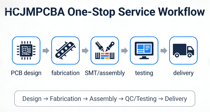
Hcjmpcba One Stop Service Workflow
In summary: a PCB is far more than a bare board — it’s the structural and electrical foundation of electronic devices. Its materials, structure, layer count, and manufacturing quality — all critically determine the performance, reliability, manufacturability and cost of end products.
For modern electronics — from consumer gadgets and wearables, to industrial control systems, medical devices, power modules and beyond — selecting the right PCB type and working with a reliable manufacturer is essential.
At HCJMPCBA, with our comprehensive capabilities, flexible production, strict quality control, and full-service model, we are ideally positioned to support global OEMs, procurement teams, and product developers. Whether you need a quick prototype, a small batch run, or mass production — we deliver high-quality PCBs and PCBA solutions tailored to your needs.
Contact us today to get your custom PCB / PCBA quote and technical consultation.
Learn how to clean battery corrosion in remote control devices and other electronics with safe, step

Discover HCJMPCBA’s 13485 medical manufacturing excellence in medical PCB assembly. Learn about me
Guangzhou Huachuang Precision Technology Co., Ltd. has achieved remarkable success in various projec


