
HCJMPCBA’s ISO 13485 Certified Medical PCB Assembly: 10+ Years of 99.99% Reliability for Life-Saving Devices
Discover HCJMPCBA’s 13485 medical manufacturing excellence in medical PCB assembly. Learn about me
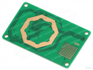
A PCB (Printed Circuit Board) is a flat board made from non-conductive materials, typically fiberglass or composite epoxy, with conductive pathways etched or printed on the surface to connect various electronic components. These boards serve as the backbone of most electronic devices, providing both mechanical support and electrical connections. Without a PCB, electronic components would be difficult to interconnect and mount.
Before the advent of PCBs, electronic circuits were constructed using point-to-point wiring, which was labor-intensive and prone to errors. The invention of the PCB revolutionized electronics by allowing for more compact, reliable, and cost-effective designs. Over time, PCBs have evolved from single-sided designs to complex multi-layer boards, accommodating the increasing demand for miniaturization and functionality in electronic devices.
A typical PCB consists of several layers:
Substrate (Base Material): The core material, usually made of fiberglass or composite epoxy, provides the mechanical structure.
Copper Layer: A thin layer of copper is applied to the substrate, which is then etched to form the conductive pathways.
Solder Mask: A layer of protective coating that prevents solder bridges and protects the copper traces.
Silkscreen: Printed markings that indicate component placements and other important information.
These materials are chosen for their electrical insulating properties, thermal stability, and mechanical strength to ensure the PCB’s reliability and performance.
PCBs come in various types, each suited for specific applications:
Single-Sided PCBs: The simplest form, with components mounted on one side and conductive pathways on the other. Common in low-density applications.
Double-Sided PCBs: Components are mounted on both sides, allowing for more complex circuits.
Multi-Layer PCBs: Consist of multiple layers of substrate and conductive material, enabling high-density circuits.
Rigid PCBs: Made from inflexible materials, suitable for applications where the board must maintain a fixed shape.
Flexible PCBs: Made from flexible materials, allowing the board to bend and fit into compact spaces.
Rigid-Flex PCBs: Combine elements of both rigid and flexible PCBs, offering versatility in design.
These types are used across various industries, including consumer electronics, automotive, medical devices, and telecommunications.
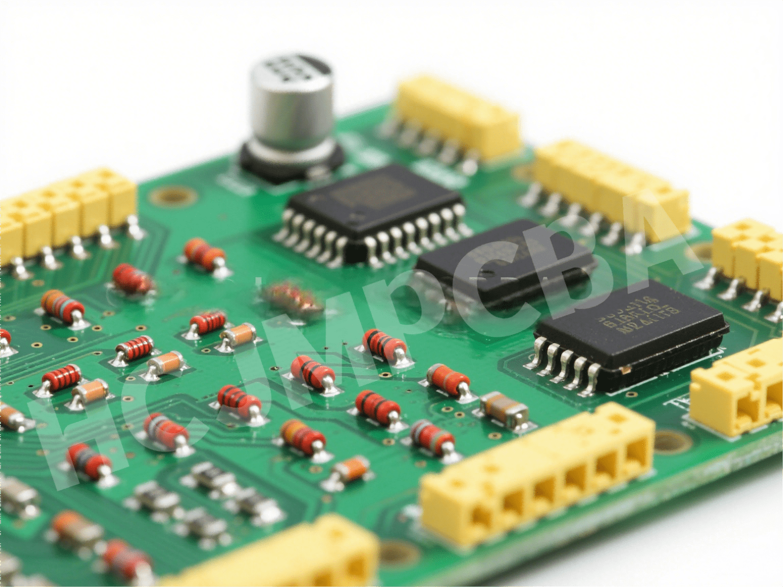
The PCB assembly process involves several steps to transform a bare PCB into a fully functional electronic circuit:
1.Design and Fabrication: The PCB design is created using CAD software, and the board is fabricated by etching the copper layer to form the desired circuit pattern.
2.Component Placement: Electronic components are placed onto the PCB, either manually or using automated machines.
3.Soldering: The components are soldered to the PCB using methods like wave soldering or reflow soldering.
4.Inspection and Testing: The assembled PCB undergoes inspection and testing to ensure functionality and quality.
5.Final Assembly: The PCB is integrated into its final product, such as a smartphone or medical device.
This process is crucial for ensuring the reliability and performance of electronic devices.
While both PCB and PCBA are integral to the electronics manufacturing process, they serve different purposes:
PCB (Printed Circuit Board): A bare board without any components. It provides the physical structure and electrical pathways for the circuit.
PCBA (Printed Circuit Board Assembly): A fully assembled PCB with all necessary electronic components soldered onto it, ready to perform its intended function.
In essence, a PCB is the foundation, while a PCBA is the completed structure that performs the desired electronic functions.
Q:What does PCB stand for in electronics?
A:PCB stands for Printed Circuit Board, a flat board used to mechanically support and electrically connect electronic components.
Q:What are printed circuit boards made of?
A:0PCBs are typically made from a combination of non-conductive materials like fiberglass or composite epoxy, and conductive materials like copper.
Q:What is the PCB assembly process?
A:The PCB assembly process involves designing the circuit, fabricating the board, placing components, soldering, inspecting, and final assembly.
Q:What is the difference between PCB and PCBA?
A:A PCB is a bare board without components, while a PCBA is a fully assembled PCB with electronic components.
Understanding what a PCB is and its role in electronics is fundamental for anyone involved in the design, manufacturing, or use of electronic devices. Whether you’re an engineer, a buyer, or a consumer, recognizing the importance of PCBs helps in appreciating the complexity and functionality of modern electronics.
Discover HCJMPCBA’s 13485 medical manufacturing excellence in medical PCB assembly. Learn about me
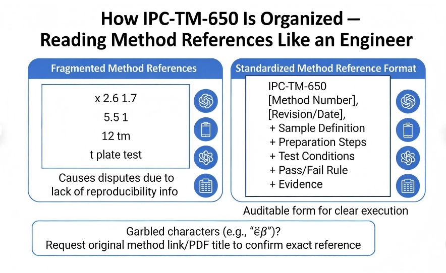
What is ipc-tm-650 and how does it help PCB and PCBA teams control quality with consistent, comparab
Guangzhou Huachuang Precision Technology Co., Ltd. has achieved remarkable success in various projec


