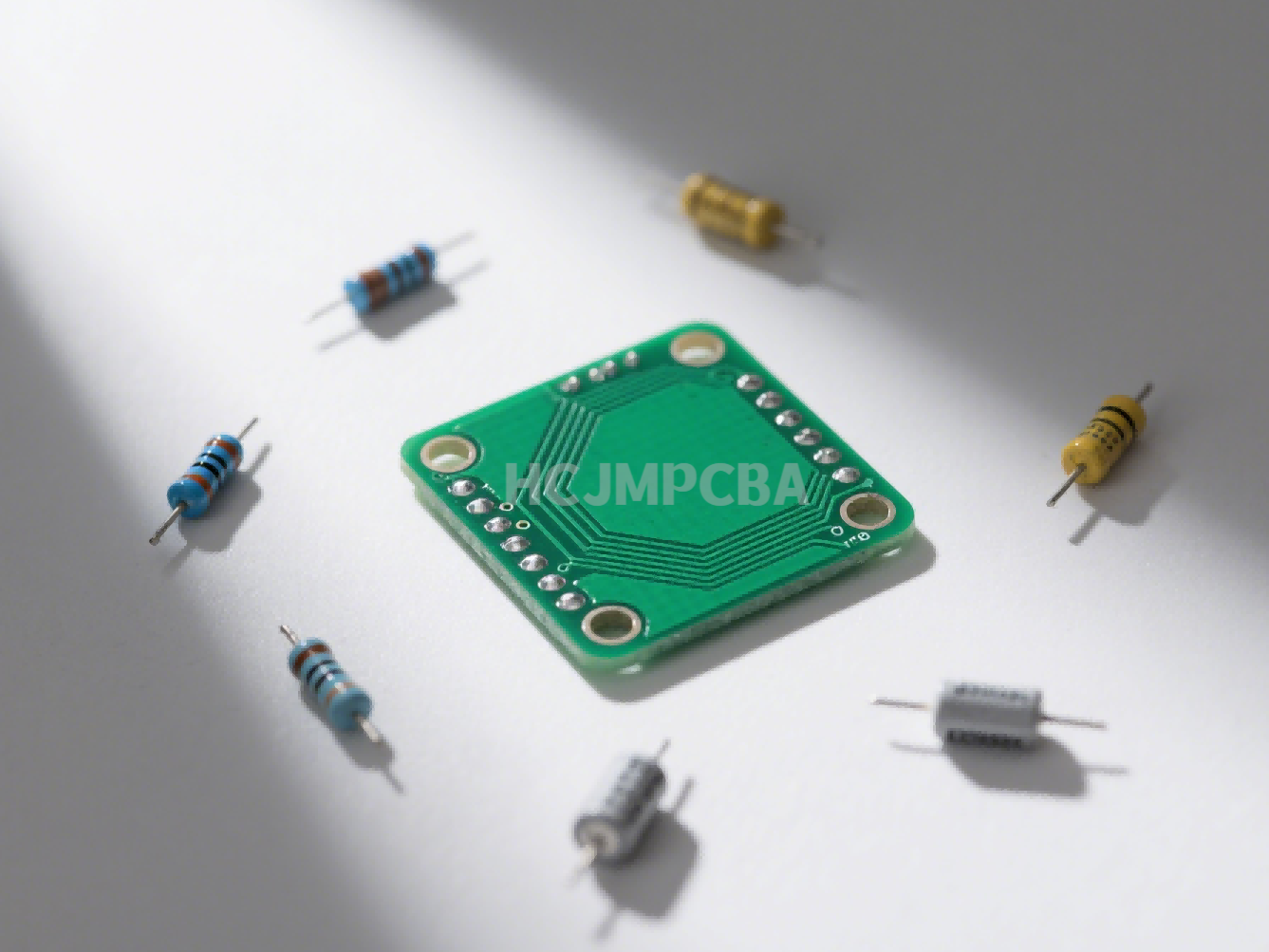
What Is a Blank PCB and Parts? Comprehensive Guide for Engineers and Buyers
Discover what a blank PCB and parts are—you'll learn about blank PCB board, bare printed circuit b
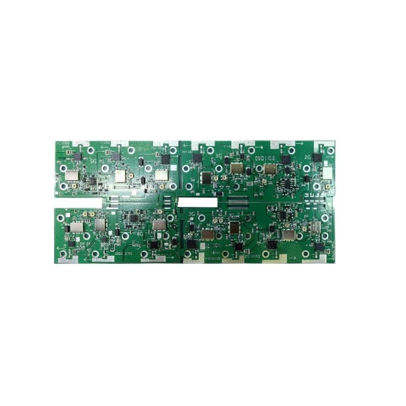
Industrial pcb production is the standardized, high-volume fabrication of multilayer boards using automated pcb manufacturing machinery to meet rigorous industrial specifications. Unlike rapid prototyping, the pcb manufacturing process at an industrial scale focuses on consistency, thermal stability, and long-term reliability. At HCJMPCBA, we integrate Design for Manufacturing (DFM) with an advanced pcb process to ensure that every printed circuit board meets IPC Class 3 standards for mission-critical applications.
1.DFM Synergy: Successful industrial pcb manufacturing requires a proactive review of Gerber files to resolve potential yield issues before the circuit board manufacturing process begins.
2.Equipment Sophistication: The use of high-precision pcb manufacturing equipment, such as Laser Direct Imaging (LDI) and Vacuum Presses, is essential for high-density interconnect (HDI) designs.
3.Accountability Through Data: Professional pcb production must be backed by raw data and a robust traceability (lot/batch/serial) system to mitigate risk in regulated industries.
The fundamental difference in industrial pcb production lies in the “Repeatability Factor.” While a hobbyist shop might focus on making one board work, an industrial pcb production process is designed to make 10,000 boards perform identically.
In a professional industrial pcb facility like HCJMPCBA, we utilize specialized pcb manufacturing machinery that monitors chemical concentrations, plating thickness, and drilling accuracy in real-time. This level of printed wiring board manufacturing process control is what separates consumer-grade electronics from industrial-grade hardware.
Designing for industrial pcb manufacturing requires a shift from “functional design” to “manufacturing design.” A board that works on a bench might fail during the pcb board manufacturing process if tolerances are too tight.
Stack-up Management: Use standard dielectric thicknesses to ensure your printed circuit board manufacturing costs remain optimized.
Copper Weight: For industrial pcb applications, 2oz copper is often required for power planes to manage thermal dissipation.
Annular Rings: Ensure the annular ring is at least 5 mils to prevent “breakout” during the high-speed drilling phase of the pcb process.

Pcb Stack Up Structure For Industrial Boards Hcjmpcba
The printed circuit board manufacturing process at HCJMPCBA is a symphony of chemical and mechanical engineering. Here is the process of pcb manufacturing broken down:
1.CAM Review & DFM: We assign a unique Method Number + Revision to your project. Our engineers analyze the Gerber files to optimize the pcb fabrication process.
2.Laminate Cutting & Preparation: Using automated pcb manufacturing machines to prepare the substrate.
3.Inner Layer Imaging (LDI): Laser Direct Imaging provides the precision required for industrial pcb manufacturing.
4.Lamination: High-pressure vacuum presses bond the layers.
5.CNC Drilling: Precision pcb manufacturing equipment drills holes as small as 0.15mm.
6.Copper Plating: The circuit board making process uses electroless copper to plate hole walls.
7.Outer Layer Imaging & Etching: Finalizing the conductive paths.
8.Solder Mask & Silk Screen: Applying protective coatings and markings.
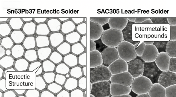
9.Surface Finish: Choosing between HASL, ENIG, or OSP for long-term solderability.
10.Electrical Testing: 100% testing of all pcb production units.
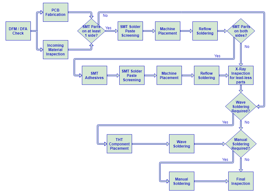
Industrial Pcb Manufacturing Process Flow Hcjmpcba
What makes HCJMPCBA a leader in industrial pcb production is our commitment to documentation and transparency.
We treat every pcb manufacturing process as a controlled experiment. Every project has a dedicated Method Number that dictates everything from oven temperature profiles to chemical dwell times. If the design is updated, the Revision code ensures the factory floor never uses outdated specs.
For mass pcb production, we follow a strict Sample Plan (ISO 2859-1). However, for mission-critical industrial pcb, we offer 100% testing. All testing is conducted under specific Test Conditions (controlled 25C temperature and 45% humidity) to ensure raw data accuracy.
We don’t just provide a “Pass” sticker. We provide raw data for impedance control and electrical continuity. This data is linked to a lot/batch/serial number. This means if you have an issue in the field, we can trace the exact pcb manufacturing machinery and raw material batch used for that specific unit.
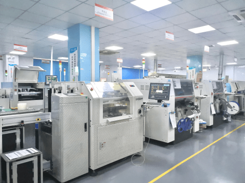
Hcjmpcba Industrial Pcb Manufacturing Equipment
1.Insufficient Thermal Relief: Large copper planes without thermal relief make soldering impossible in the pcb board manufacturing process.
2.Missing Fiducials: Automated pcb manufacturing equipment needs fiducial markers for alignment.
3.Via-in-Pad without Plugging: This leads to solder wicking and weak joints in the pcb process.
4.Inconsistent Drill Sizes: Using too many different drill sizes increases pcb manufacturing time and cost.
5.Ignoring Edge Clearance: Placing traces too close to the board edge results in exposed copper during the routing stage of circuit board manufacturing process.
Q: What is the lead time for mass industrial pcb production?
A: Standard mass production typically takes 10-15 working days, depending on the complexity of the pcb manufacturing process and material availability.
Q: How does pcb manufacturing machinery affect quality?
A: High-end pcb manufacturing machines like LDI eliminate the “film-stretch” issues common in manual photolithography, ensuring $100\%$ alignment accuracy.
Q: Can I use hobbyist design software for industrial pcb?
A: While possible, we recommend professional tools (Altium, Allegro) that allow for better printed circuit board manufacturing output files (ODB++ or Gerber X2).
Q: How do you handle lot/batch/serial traceability?
A: We laser-mark a unique QR code on every printed circuit board. This code links back to our ERP system where raw data is stored.
Procurement managers, use this clause to protect your supply chain:
Choosing a partner for industrial pcb production is about choosing a partner in risk management. At HCJMPCBA, our blend of high-precision pcb manufacturing machinery and rigorous data-logging ensures that your design is realized with zero compromise.
For more information about PCBA services, please contact Guangzhou Huachuang Precision Technology(HCJMPCBA).
Update triggers: standard revision changes / recurring questions / production checklist updates.
Discover what a blank PCB and parts are—you'll learn about blank PCB board, bare printed circuit b
Learn kicad how to draw curved coplanar waveguide with ground plane backing to achieve precise imped
Explore the PCB Manufacturing Process from design and imaging to etching, drilling, plating, and fin