
How to Read the Resistor Color Code?
Learn how to read the resistor color code with our step-by-step guide. Decode 4-band and 5-band resi

In today’s competitive electronics market, businesses in North America and Europe constantly seek reliable pcb design services to ensure their products meet high standards of performance, manufacturability, and regulatory compliance. Whether you’re searching for circuit board design service, pcb layout services, or custom pcb design services, understanding the fundamentals of pcb design services is vital.
From CAD schematics to Gerber outputs, the journey of pcb design spans disciplines including electrical, mechanical, and test engineering. This article provides a systematic, how-to overview, explaining “what file type is used for pcb designs,” “what is pcb design and how to design a pcb,” and how to engage printed circuit board design services effectively.
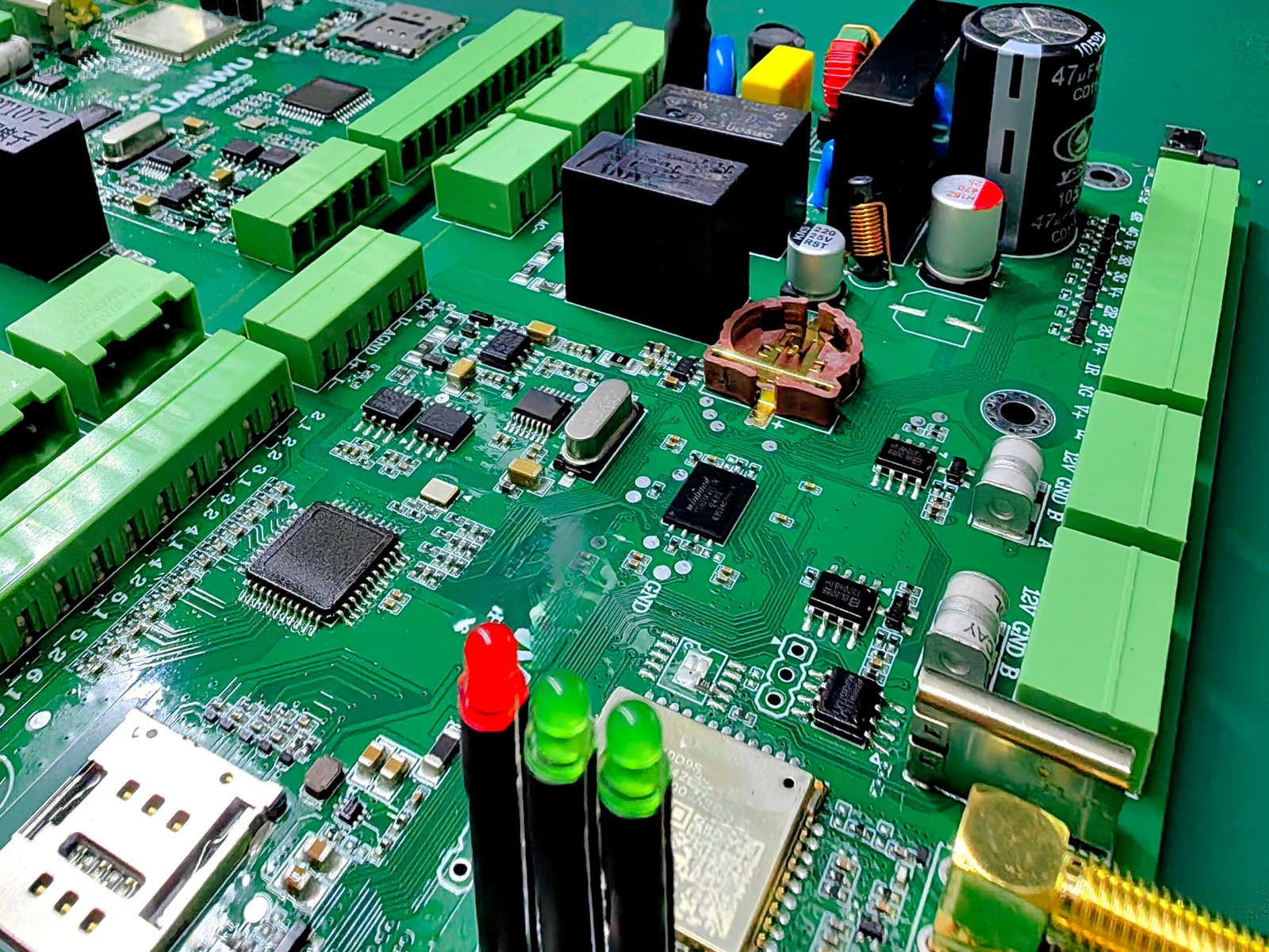
PCB design services refer to the complete process of creating a printed circuit board—from conceptualizing the circuit and schematic draft to layout, validation, and file output for manufacturing. It integrates pcb layout services, schematic design services, and printed circuit board layout services, ensuring that circuit boards are both functional and manufacturable.
In essence, printed circuit board design services provide clients with a seamless path from ideas to physical boards ready for pcb design and fabrication.
Understanding what file type is used for pcb designs is fundamental for designers and decision-makers.
Gerber files are the de facto standard for PCB fabrication—used to depict copper layers, solder mask, legend, and more.
ODB++ is a comprehensive format that includes layout, drill data, component placement, BOM, and netlist—streamlining integration between design and manufacturing.
These files convey precise hole positioning and size for drilling, often in Excellon format, and are required in addition to Gerbers.
.sch files capture electrical connectivity in schematic capture tools like OrCAD, Altium, or KiCad.
.kicad_pcb files store layout data in KiCad projects.
Proprietary project files (.pcbdoc, .pcb) also store design data for editing and simulation.
IPC-2581: smart data format for fabrication;
Bill of Materials (BOM) and Pick-and-Place (Centroid / CPL) files for assembly.
Here’s a structured explanation, from a professional perspective, outlining how to design a PCB using pcb design services.
Clarify electrical parameters, board size, operating environment, and functionality. A clear high-level block diagram aids the process.
Use PCB design or schematic design services to draft the circuit logic. This includes selecting components, defining interconnections, and building the BOM—all foundational to PCB layout.
Choose layer count (e.g., 2-layer, 4-layer), material, impedance control, and special board features.
Assign accurate footprints, then position components strategically for routing efficiency, thermal management, and EMI control.
Connect pads using optimized trace routing, define power & signal layers, and maintain signal integrity with design rules (DRC/DFM).
Perform layout reviews to detect stack-up issues, insufficient spacing, or DRC violations.
Generate Gerber, drill, BOM, pick-and-place, and optionally ODB++ or IPC-2581 files.
Send final deliverables to manufacturers or pcb design companies; integrate DFM feedback for seamless production.
Common file types include:
Gerber (RS-274X/X2/X3)
ODB++
Drill (NC Drill / Excellon)
Schematic (.sch), layout files (.kicad_pcb, .pcbdoc)
BOM, Pick-and-Place (Centroid), IPC-2581
These formats are essential to pcb layout services, printed circuit board design services, and further enable efficient pcb design and fabrication.
Professional pcb design services ensure robust designs, compliance, manufacturability, and risk minimization.
Outsourcing to pcb designers reduces time-to-market and avoids rework.
Partnering with firms certified to ISO 9001 ensures quality assurance and continuous improvement. Though not yet searched, it’s best practice to work with iso 9001 certification companies for design reliability.
Custom or outsourced pcb design and layout services adapt to client project scopes, from prototype to large-scale manufacturing.
Popular EDA tools include:
KiCad: open-source, schematic capture, layout, Gerber output.
Altium Designer, OrCAD: professional suites with DRC, simulation, and collaboration.
Adherence to IPC and ISO 9001 ensures reliable design practices.
Use of iso 9001 certification companies for design and documentation enhances trust.
Q: What file type is used for PCB designs?
A: Typical files include Gerber (RS-274X/X2/X3), ODB++, NC Drill, schematic files (.sch), layout files (.kicad_pcb), BOM, pick-and-place, and IPC-2581.
Q: How does a PCB design service work?
A: A service provider receives your schematic or requirements, designs the layout, runs DRC/DFM checks, and provides manufacturing-ready outputs (Gerber, BOM, pick-and-place).
Q: What defines a good PCB design?
A: A good PCB design balances functional performance, manufacturability, signal integrity, thermal management, and cost-efficiency.
Q: What’s the difference between PCB design and layout?
A: PCB design refers to schematic creation and planning. PCB layout is the physical arrangement—component placement and routing.
Mastering pcb design services allows OEM engineers, procurement specialists, and end users across North America and Europe to confidently transition from concept to reality. A sound workflow spans defining requirements, schematic capture, layout, review, and producing accurate manufacturing files like Gerber and BOM.
For reliable, high-quality pcb design and fabrication, work with established providers who adhere to industry standards and use powerful EDA tools such as KiCad or Altium.
Learn how to read the resistor color code with our step-by-step guide. Decode 4-band and 5-band resi
Discover what does PCB stand for in this comprehensive guide by HCJMPCBA. Learn about ict tester rol

Explore the fundamentals of circuit board design, from schematic creation to layout and manufacturin


