1. Introduction
SMT, or smt meaning in electronics, stands for Surface Mount Technology—the dominant method today for placing surface-mount electronic components directly onto printed circuit boards without traditional through-hole leads. Understanding what is smt technology and the detailed smt process is critical for OEM engineers, purchasing managers, and clients who want to improve efficiency, reduce cost, and achieve compact, high-density smt circuit boards.
This comprehensive guide explains the full SMT workflow, essential equipment, best practices, and challenges—all designed to help you grasp SMT fundamentals and evaluate suppliers like HCJMPCBA effectively.
2. What Is SMT? Definition and Evolution
Surface Mount Technology (SMT) refers to the method of assembling electronic components—known as Surface Mount Devices (SMDs)—directly onto the surface of a PCB, bypassing the need for drilling holes. (This definition meets the smt meaning in electronics intent.) SMT replaced older through-hole techniques because it enables automation, miniaturization, and significantly higher component densities.
First developed in the 1960s and completed mature adoption by the late 1990s, SMT became dominant due to its efficiency and design flexibility. Early implementations by IBM paved the way for the modern electronics era.
3. Core SMT Components & Equipment
3.1 Surface Mount Devices (SMDs)
Components designed for SMT—such as resistors, capacitors, transistors, LEDs, and ICs like QFP and BGA—are collectively known as surface-mount electronic components or SMT components.
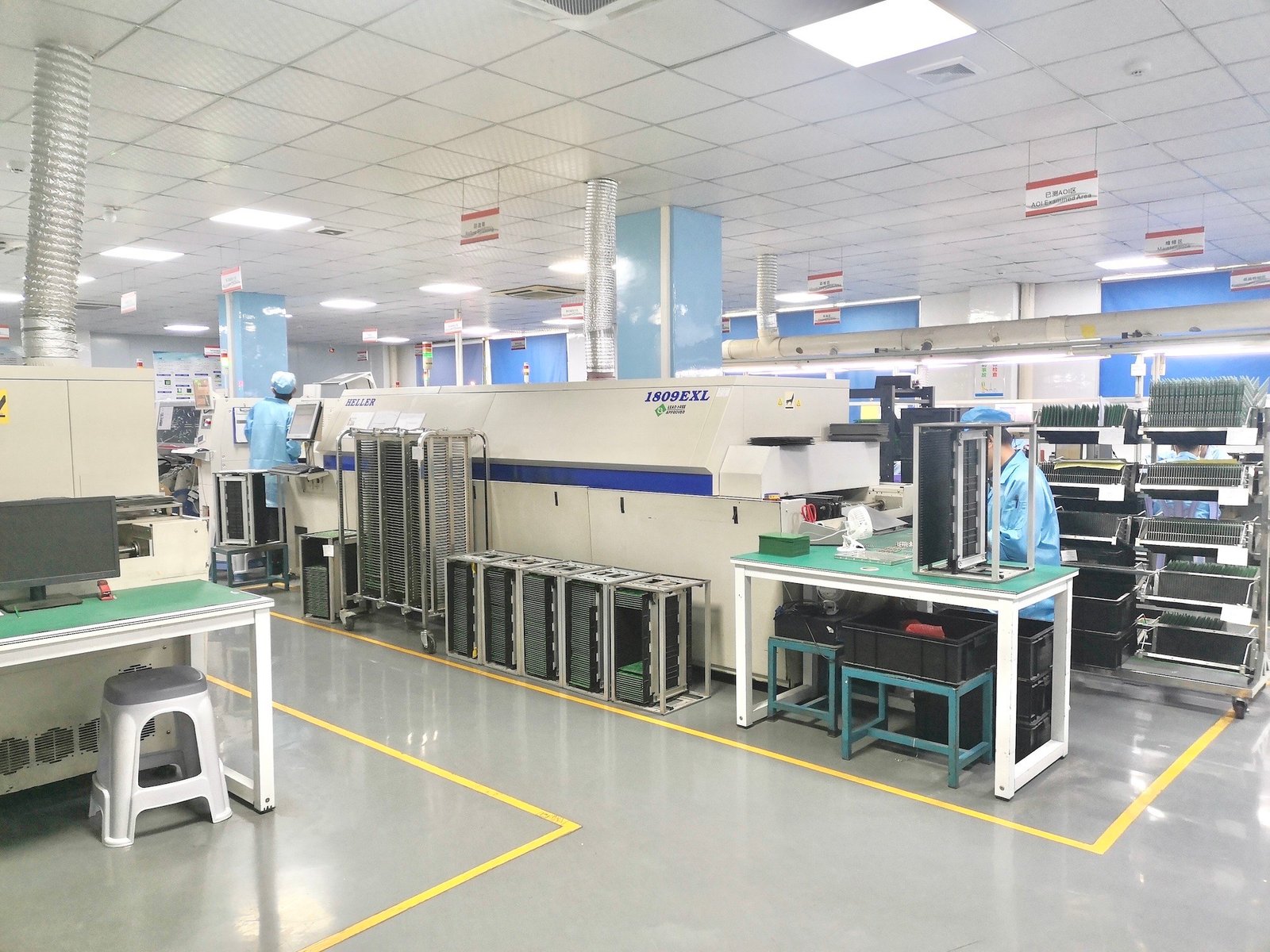
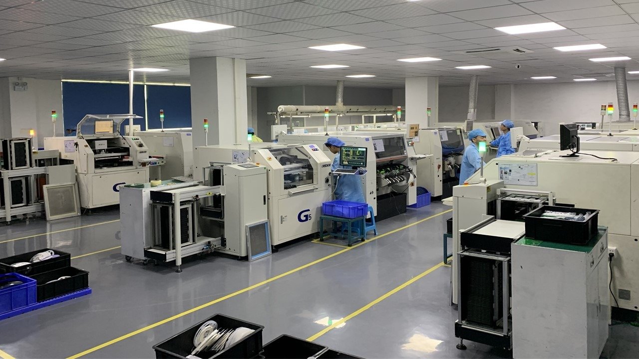
3.2 SMT Equipment
Successful SMT implementation relies on several specialized machines:
(1)Solder Paste Printer: Applies paste to PCB pads via a precise stencil.
(2)Solder Paste Inspection (SPI): Scans paste deposits for consistency using 2D or 3D inspection systems.
(3)Pick-and-Place Machine: Places components at high speed and accuracy using robotic heads and vision systems.
(4)Reflow Oven: Applies a thermal profile to melt the solder paste and solidify component bonds (typical lead-free profile peaks around 217 °C for SAC305).
(5)Inspection Systems: AOI, X-ray, or manual checks ensure joint integrity and detect defects.
4. SMT Process: Step-by-Step Workflow
A robust SMT process typically includes:
4.1 Pre-Production Preparation
Review design files (Gerber, BOM, coordinate data), inspect incoming parts, and fabricate the stencil.
4.2 Solder Paste Printing
Paste is applied using a stencil; precise alignment via fiducials ensures accuracy.
Paste quality, stencil specifications (thickness ~0.12 mm), squeegee angle (~45°), speed (30–50 mm/s), and print quality are critical.
4.3 Solder Paste Inspection (SPI)
Real-time checks using SPI detect inaccuracies in volume or alignment, reducing downstream defects.
4.4 Component Placement
Operator-assisted or automated placement ensures precise mounting. Placement relies on tape feeders or trays and advanced vision systems.
High-speed machines support up to 80,000–200,000 components/hour.
4.5 Reflow Soldering
The PCB passes through thermal zones: preheat, soak, reflow (peak ~217 °C), and cooling control joint formation.
4.6 Post-Reflow Inspection & Testing
Use AOI and X-ray to identify solder defects. For high volume, ICT and functional testing confirm PCB reliability.
4.7 Back-End Processing
Includes rework, cleaning, depanelization, packaging, and ESD-safe storage.
5. Benefits of SMT for OEMs & Procurement
(1)Higher Component Density & Miniaturization — SMT enables compact, double-sided design where through-hole cannot.
(2)Cost & Time Efficiency — Automated processes reduce labor, speed up production, and shorten lead times.
(3)Improved Electrical & Mechanical Performance — Shorter interconnects reduce parasitic effects and enhance vibration reliability.
(4)Scalability and Reliability — From prototype to mass production, SMT adapts seamlessly with high first-pass yield.
(5)Material & Space Optimization — Supports high-frequency, HDI, and multi-layer boards.
6. Design Guidelines & Best Practices
(1)Stencil & Paste Control: Match stencil aperture with component size to avoid paste misplacement.
(2)Paste Management: Store in a refrigerator; avoid using exposed paste after two hours.
(3)Thermal Profiling: Optimize ramp, soak, peak, and cooling to avoid tombstoning or voiding.
(4)Inspection Integration: Include SPI, AOI, and X-ray within the production flow to catch defects early.
(5)Hybrid Boards: Use selective soldering for through-hole components when necessary.
7. Challenges & Mitigation Strategies
(1)Fine-Pitch Placement – Requires precise machines and high-resolution vision systems.
(2)Thermal Damage – Poor profiling leads to part damage or warpage.
(3)Rework Complexity – SMT repairs require thermal-controlled tools and experienced operators.
(4)Hybrid Design Complexities – Combining SMT and THT increases routing and assembly complexity.
8. SMT vs Through-Hole Technology
| Feature |
SMT (Surface Mount Technology) |
Through-Hole Technology |
| Component Placement |
Surface-mounted (high density, both sides) |
Leads through drilled holes |
| Assembly Speed |
High-speed automation |
Slower, often manual |
| Reliability |
High electrical reliability |
Stronger mechanical retention |
| Cost & Efficiency |
Low labor, scalable |
Higher labor and production costs |
| Ideal Applications |
Compact, automated electronics |
Power connectors, heavy-duty modules |
9. Where to Buy SMT Services & Equipment
When evaluating what is an smt machine, or seeking surface mount technology equipment, look for:
(1)Certified SMT lines with SPI, AOI, and reflow capabilities
(2)Skilled smt operator support and process documentation
(3)Quality standards, transparent pricing, and box build assembly process capability
At HCJMPCBA, we offer turnkey SMT production line services, combining advanced machines with experienced staff to deliver reliable, high-density pcb smt assembly solutions.
10. FAQs (QFA)
Q: What does SMT mean?
A: SMT stands for Surface Mount Technology, meaning electronic components are placed on the surface of a PCB rather than through holes
Q: How does the SMT process work?
A: It involves solder paste printing → SPI → component placement → reflow soldering → inspection/testing.
Q: What constitutes SMT equipment?
A: Includes paste printers, SPI, pick-and-place machines, reflow ovens, and inspection systems.
Q: Why prefer SMT over through-hole?
A: Offers higher density, better electrical performance, automation compatibility, and cost savings.
Q: Can SMT and through-hole coexist?
A: Yes—hybrid PCBs combine both technologies, using selective soldering for THT parts while optimizing layout for SMT efficiency.
11. Conclusion
Understanding SMT, along with its meaning, process, equipment, design practices, advantages, and challenges, is essential for professionals in PCB SMT, prototyping, and high-volume assembly. Surface Mount Technology continues to drive innovation, enabling compact, efficient, and reliable electronics.
To learn more about PCBA services, please contact Guangzhou Huachuang Precision Technology.