Understanding the PCB manufacturing process is key for anyone working in printed circuit board production. From raw design files to finished boards, mastering each stage ensures high yield and reliability. Here’s how HCJMPCBA—your trusted services partner—delivers flawless results.
1. From Schematic to DFM-Friendly Design
Initial design starts with schematic capture and PCB layout using CAD tools like Altium or KiCad. Outputs include Gerber or IPC-2581 files essential for printed wiring board manufacturing process. At HCJMPCBA, each design undergoes comprehensive Design-for-Manufacturability (DFM) checks to match our fabrication capabilities and avoid downstream issues.
2. Film Plotting or Laser Direct Imaging
The finalized Gerber data is converted into photo films for each copper layer, solder mask, and silk — essential for accurate pattern transfer. Some facilities use Laser Direct Imaging (LDI) for higher precision. HCJMPCBA supports both methods as part of our pcb manufacturing techniques.
3. Inner-Layer Etching & Multi-Layer Lamination
Copper-clad substrates (usually FR-4) are coated with photo-resist and exposed to UV through aligned films. Unprotected copper is then etched away. Layers are optically punched into perfect registration before laminating multiple stacks using heat and pressure—forming multilayer boards.
4. Precision Drilling and Copper Plating
CNC drilling machines create thru‑holes, microvias, and mounting holes. Registration accuracy is crucial. After drilling, through-hole plating connects layers by depositing copper within holes. Then, surface finish options like ENIG, OSP, or HASL are applied for solderability and oxidation resistance.
5. Solder Mask and Silkscreen Application
A solder mask layer is applied to insulate exposed copper traces and prevent shorts during aggregation. Then silkscreen (legend printing) adds component designators, logos, and test points to the boards—critical for assembly and post-production handling.
6. Bare-Board Electrical Testing
Before PCB assembly, the bare board undergoes electrical testing for opens and shorts—using flying-probe or bed-of-nails testers depending on volume. This step ensures functionality before populating the board with components.
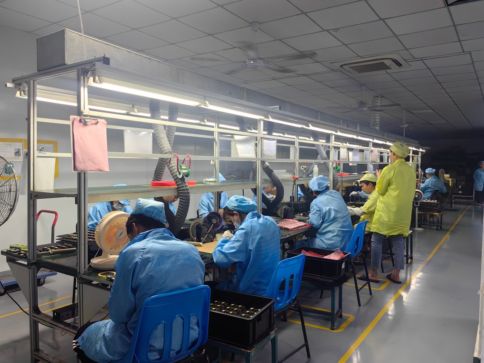
7. PCB Assembly: SMT, Reflow & Inspection
7.1 Solder Paste Printing & Component Placement
Solder paste is applied with stencils, checked by SPI, then components are placed using pick-and-place machines that achieve ±5 µm precision. HCJMPCBA holds IPC-A-610 Class 2/3 certifications for reliable placement accuracy in high‑density boards.
7.2 Reflow or Wave Soldering
Reflow ovens with nitrogen control produce optimal solder joints for SMT components. Through-hole parts may use wave soldering if included in the design. Process control ensures minimal thermal stress and consistent connections.
7.3 Inspection & Functional Testing
HCJMPCBA’s final inspection and functional testing go far beyond visual checks:
After reflow soldering, boards undergo Automated Optical Inspection (AOI) to catch surface-level defects like solder bridging, missing or misaligned parts, polarity errors, and insufficient fillets. AOI systems provide fast, reliable defect detection and yield repeatable results—even integrating machine learning to reduce false positives over time.
Critical components such as BGA or QFN packages then receive X‑Ray inspection (AXI). This non‑destructive method uncovers hidden faults like internal solder voids, cold joints, or layer misalignments—issues AOI cannot detect. AXI is essential for high-reliability electronics and helps ensure structural integrity under demanding conditions.
Beyond AOI and X‑Ray, each board undergoes functional testing (FCT or ICT)—a simulation of real-world operation. This may include signal flow checks, voltage response, communication protocol adherence, or integrated power delivery testing. Functional testing confirms the board performs as intended in its final application, reducing costly field failures or customer returns.
Our quality framework logs test results per unit, enabling full traceability and data-driven quality improvement—helping HCJMPCBA deliver flawless performance across pcb manufacturing process and PCBA assembly.
Why Knowing the PCB Manufacturing Process is Vital
For procurement engineers and OEM decision-makers, understanding each pcb manufacturing step helps select suppliers, anticipate lead times, and minimize defects. HCJMPCBA’s expertise in both pcb board production and post-assembly PCBA ensures design alignment and consistent output.
A successful pcb manufacturing process hinges on design foresight, precise fabrication, and robust QC. HCJMPCBA combines advanced techniques, rigid process control, and exceptional craftsmanship across pcb production process and pcb fabrication process to deliver boards that perform.
Interested in exploring case studies or diving deeper into our process capabilities?
Contact us to learn more about HCJMPCBA’s superior PCBA services.