7-Fundamental Stages of the PCB Manufacturing Process: A Precision Guide by HCJMPCBA
Explore the PCB Manufacturing Process from design and imaging to etching, drilling, plating, and fin
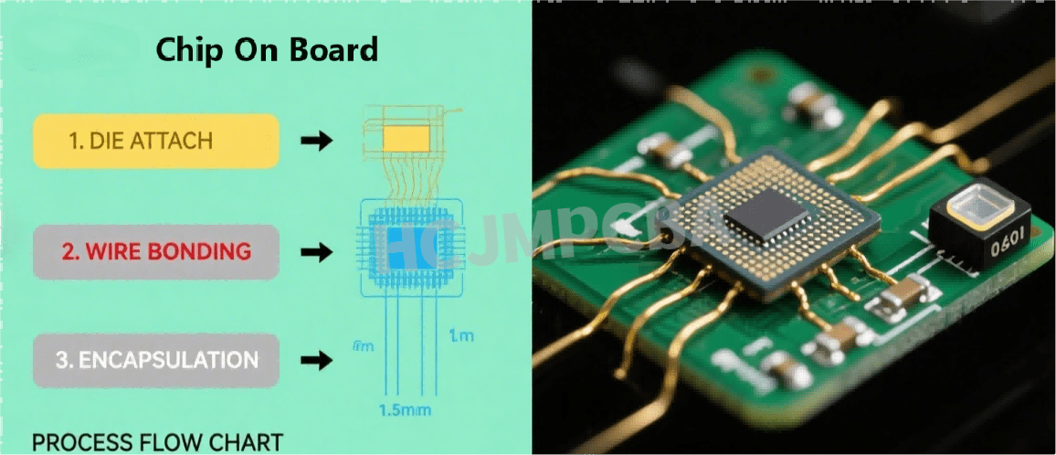
A Chip On Board (COB) is an advanced packaging technique in which unpackaged semiconductor dies (bare chips) are attached directly to a printed circuit board (PCB), electrically connected (via wire bonds or flip-chip), and then sealed with an epoxy or protective encapsulant—often referred to as a “glob top”. By merging component packaging and PCB mounting into one step, COB effectively acts as a “level 1.5 packaging” solution.This method minimizes cost, size, and weight, while improving performance in applications requiring high integration.
COB has emerged as essential technology for modern PCBA (Printed Circuit Board Assembly) for several compelling reasons:
2.1Miniaturization – Eliminates traditional IC packaging overhead, reducing footprint by 30–50%, enabling compact form factors.
2.2Enhanced Electrical Performance – Shorter signal paths significantly reduce parasitic capacitance and inductance, improving performance in RF and high-speed circuits.
2.3Better Thermal Efficiency – Direct die-to-board contact and epoxy encapsulation facilitate improved heat dissipation.
2.4Lower Cost – Avoidance of individual chip packaging reduces both materials and processing costs, especially in high-volume production.
Here is a structured overview of the chip on board process, presented in professional sequence:
3.1Substrate Preparation
The PCB is cleaned and treated—often with ENIG or electroplated gold—to enhance die adhesion and reliability of connections.
3.2Die Attach
The bare semiconductor die is positioned precisely on the PCB using conductive or non-conductive adhesives such as silver-filled epoxy.
3.3Electrical Interconnection
Wire Bonding: Using gold or aluminum wire, fine connections are made between chip pads and PCB traces.
Flip-Chip: Alternatively, the chip is flipped and solder bump connected to the board, followed by reflow.
3.4Encapsulation
The bonded area is sealed using epoxy glob-top or dam & fill techniques, protecting the die and wires from damage, moisture, and contaminants.
3.5Testing & Inspection
Electrical tests and visual inspections verify functionality and integrity. COB requires careful quality control due to its sensitive nature.
4.1Ultra-Compact Design
COB packaging achieves one of the smallest footprints by doing away with bulky IC shells.
4.2Superior Electrical & Thermal Performance
Direct connections and encapsulation materials reduce electromagnetic interference and heat buildup.
4.3Cost Efficiency in High Volume
Consolidated packaging saves cost via material reduction and simplified manufacturing.
4.4Robustness & Reliability
Encapsulation improves resistance to mechanical shock, vibration, moisture—ideal for harsh environments.
4.5Ideal for IoT and LED
COB is widely used in LED lighting modules and compact electronics like wearables due to its miniaturization and bright, reliable performance.
COB offers a more compact design and improved thermal/electrical performance, though repair and rework are harder. SMT is easier for automated assembly and mass production.
BGA provides high I/O density and better protection but at higher cost and complexity. COB is cost-effective and compact but less repairable.
Flip-chip supports high connectivity but requires complex substrate layers. COB is simpler, relying on wire-bonding, but has lower I/O density.
DIP is easy to prototype but bulky; COB excels in compact, durable applications like LED modules or automotive sensors.
6.1LED Lighting: COB LEDs offer superior brightness and thermal efficiency; widely used in cabinetry lighting, automotive lights, and general illumination.
6.2Wearables & IoT Devices: COB enables tiny, powerful modules critical for smartwatches, sensors, and compact electronics.
6.3Automotive Electronics: Stability in temperature extremes and vibrations makes COB suitable for sensors and controllers.
6.4Medical & Industrial Equipment: COB’s reliability and compactness are leveraged in diagnostic and instrumentation gear.
6.5RF & High-Frequency Circuits: Minimal signal distortion benefits RF modules and advanced communications hardware.
To ensure robust assembly and performance, professionals must consider:
7.1Surface Finish: Use ENIG or thick gold plating to improve die adhesion and wire bond reliability.
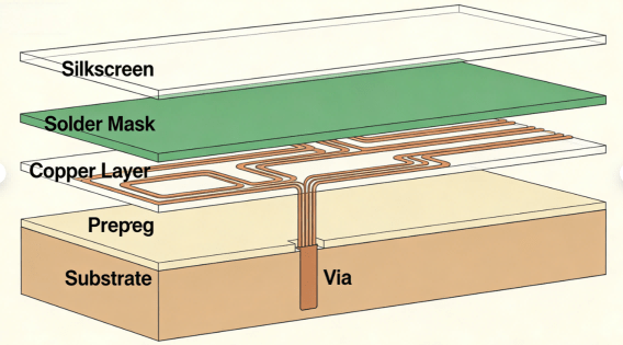
7.2Via Avoidance: Avoid vias under encapsulated areas—or ensure they are fully plugged—to prevent encapsulant leakage.
7.3Fiducial Marks: Include cross-shaped alignment marks to aid automatic die placement.
7.4Pad Design: Pads should slightly exceed die dimensions (by ~0.25–0.3 mm) to minimize placement errors and rotational drift.
7.5Wire Bond Management: Ensure consistent bond lengths and avoid diagonal wiring to reduce short-circuit risk.
7.6Encapsulation Strategy: Optimize dam & fill or glob-top methods to protect while managing stress and heat effectively.
7.7Cleanroom Standards: Die attach and bonding often require cleanroom conditions (Class 10,000 or better).
Q: What is the difference between “chip on board” and “PCB chip”?
A: “Chip on board” refers specifically to the COB packaging process. “PCB chip” is a generic or misused variation. Both relate to die-on-board concepts but COB is precise.
Q: How to make a chip on board?
A: Follow the structured chip on board process above: substrate prep → die attach → wire bonding or flip-chip → encapsulation → testing.
Q: What is COB LED?
A: COB LED integrates multiple chip dies on a PCB substrate and encapsulates them to form a compact light module. It offers improved thermal and electrical efficiency.
Q: What is the difference between PCB and COB?
A: PCB is the board itself; COB involves mounting the bare die directly onto the PCB for higher integration and efficiency.
9.1Chip on board (COB) is a highly efficient packaging technique that delivers compact size, improved thermal and electrical performance, and lower cost by mounting bare chips directly onto PCBs.
9.2The detailed chip on board process involves die attach, interconnection via wire bonding or flip-chip, encapsulation, and testing.
9.3COB outperforms traditional methods like SMT, BGA, and DIP when compactness and performance are priorities.
9.4It’s widely used in LED modules, wearables, automotive electronics, medical systems, IoT, and RF devices.
9.5Proper PCB design and clean manufacturing are critical for reliable COB deployment.
For tailored PCB/PCBA OEM solutions, choose HCJMPCBA. Our expertise in COB processes, secure manufacturing, and global supply chain ensures your product is compact, efficient, and high-quality.
Explore the PCB Manufacturing Process from design and imaging to etching, drilling, plating, and fin
Direct Answer The global resistor and capacitor market in 2026 is no longer a stable commodity envir
What is a PCB printed circuit board? This guide explains the definition of PCB, the parts of a PCB b