CTA
Update triggers: standard revision changes / recurring questions / production checklist updates.
A low pass filter (low-pass filter) is an electronic network that passes signals below a chosen cutoff frequency while reducing signal content above that cutoff. It is used to remove high-frequency noise, shape bandwidth (for example in low pass filter audio paths), and prevent aliasing ahead of analog-to-digital conversion.
This guide is maintained by the HCJMPCBA engineering team and updated with production checklists.
1.A low-pass filter is defined by measurable targets: cutoff frequency (often the “-3 dB point”), roll-off slope (filter order), passband loss, and phase/group delay—not by “a capacitor somewhere.”
2.Real hardware performance depends on source impedance, load impedance, and layout parasitics; these can shift cutoff frequency and add resonance.
3.Reliable projects specify verification evidence up front: method number + revision, sample plan, test conditions, raw data, and traceability (lot/batch/serial).
A low pass filter reduces high-frequency components in a signal while preserving lower-frequency content. Engineers use it to:
Smooth sensor outputs and reduce noise pickup on a circuit board device.
Limit bandwidth to reduce electromagnetic interference (EMI) and susceptibility.
Create anti-aliasing behavior before an ADC (analog-to-digital converter).
Shape frequency response in audio and amplifier systems (low pass filter on amplifier paths can limit hiss, switching noise, or unwanted high-frequency artifacts).
In plain terms: it acts like a controlled “frequency gate.” Low frequencies pass with minimal attenuation; higher frequencies are increasingly attenuated beyond the cutoff.
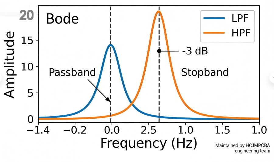
A low-pass filter keeps low frequencies and attenuates high frequencies.
A high-pass filter keeps high frequencies and attenuates low frequencies.
They are complementary tools and can be combined into band-pass and band-stop networks.
What Does A Low Pass Filter Do
Cutoff frequency (fc) is commonly defined as the point where the output amplitude drops by 3 dB relative to the passband (about 0.707× the voltage level). In a practical low pass filter circuit, the exact “effective cutoff” also depends on source and load impedance, component tolerances, and parasitic elements.
Filter “order” describes how aggressively the filter attenuates beyond cutoff. A higher order filter typically provides a steeper slope, which helps when you must strongly reject a narrow band of interference. However, higher order also tends to increase sensitivity to tolerance, layout parasitics, and may introduce phase distortion or ringing—especially in LC designs.
A frequent reason a lowpass filter works in simulation but not on hardware is that the simulated source and load are ideal. In real systems:
The source has output impedance.
The next stage (amplifier input, ADC input network, cable, etc.) presents a load.
These impedances interact with RC/LC networks and can shift the cutoff frequency or reduce attenuation in the stopband.
Use the table below to select an approach based on application, frequency range, and constraints. (This also helps procurement align expectations.)
| Application | Typical Target Cutoff | Source/Load Sensitivity | Recommended Topology | Typical Order | Key Risks | Verification Priority |
|---|---|---|---|---|---|---|
| Low pass filter audio (preamp, DAC output, active speakers) | 5 kHz–30 kHz | Medium | Active op-amp LPF or RC with buffer | 1–4 | Phase shift, op-amp bandwidth limits | Response + noise + THD (if applicable) |
| Sensor anti-aliasing before ADC | fc below Nyquist margin | High | RC + buffer or active LPF | 1–2 | Aliasing if fc too high; loading shifts | fc accuracy + phase/group delay |
| EMI reduction / switching noise shaping | kHz–MHz (depends) | Medium–High | RC snubbers, LC, or multi-stage | 1–3 | Resonance, layout parasitics | Attenuation at noise bands + stability |
| Power/drive outputs (higher current) | kHz–100 kHz+ | Medium | LC (passive low pass) | 2–3 | Resonance, component ESR/heat | Stopband attenuation + thermal behavior |
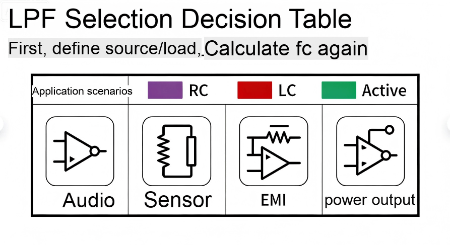
Illustration Of Lpf Selection Decision Table
Write the requirements in measurable terms:
Desired passband (what frequencies must remain).
Noise/interference frequencies to attenuate (switching ripple, RF pickup, clock harmonics).
Allowable passband attenuation (insertion loss).
Allowable phase shift or group delay (especially for audio and control loops).
Expected source and load impedance (or specify “must be buffered”).
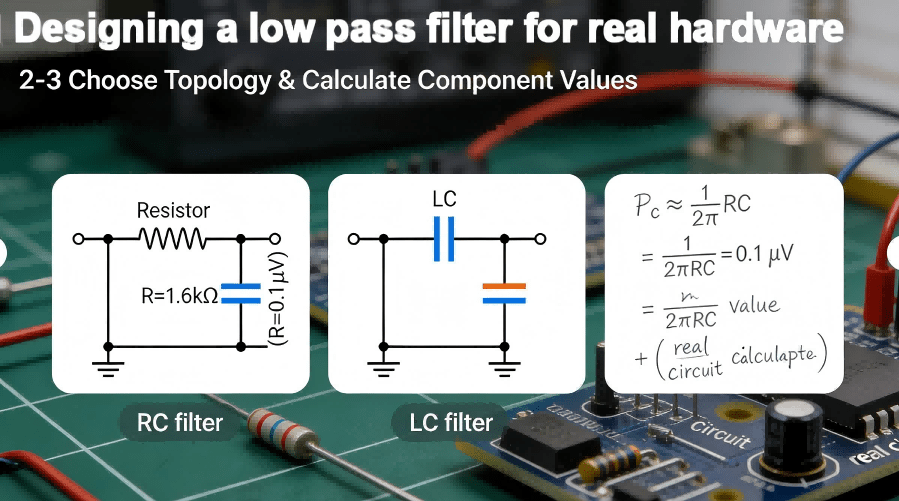
RC low pass filter: simplest, low cost, but strongly affected by load.
LC low-pass filter: lower loss at higher power, but can resonate and is layout sensitive.
Active low-pass filter: uses an op-amp (or active stage) to reduce loading sensitivity and shape response, but requires power and proper stability/bandwidth selection.
For a first-order RC low pass filter:
fc≈12πRCf_c \approx \frac{1}{2\pi RC}
Example: if you want ~1 kHz cutoff and choose R = 1.6 kΩ, then:
C≈12π⋅1600⋅1000≈0.1μFC \approx \frac{1}{2\pi \cdot 1600 \cdot 1000} \approx 0.1 \mu F
This is a starting point only. In real circuits, the effective R and C can change due to loading, input capacitance of the next stage, and parasitic capacitance/inductance on the pcb electronics layout.
For LC low pass filter design (a passive low pass), you often start from a known prototype (Butterworth/Chebyshev families) and then map values to your cutoff frequency and impedance environment. A common mistake is to pick an “example passive 100 kHz low-pass LC filter” from a calculator without matching the real source/load impedance and without validating resonance and component ESR.
In practice, for LC filters:
Confirm the intended impedance (for example 50 Ω vs 75 Ω vs “unknown and variable”).
Select inductor and capacitor with appropriate current rating, voltage rating, ESR, and tolerances.
Expect layout to change behavior above tens to hundreds of kHz if the layout is loose.
Do not stop at ideal simulation. Add:
Component tolerances (±1%, ±5%, ±10%).
Capacitor ESR/ESL, inductor DCR, parasitic capacitance of nets.
Source and load models.
Output to save (and later verify): response plots and tolerance bands that become acceptance criteria.
A breadboard low pass filter is helpful for low-frequency demonstrations, but it can mislead for higher-frequency designs because:
Breadboards add parasitic capacitance and inductance.
Lead lengths create unintended resonant networks.
For any design sensitive above a few kHz to tens of kHz (and certainly for EMI/switching noise), a small PCB prototype is the safer validation method.
Treat the filter as a controlled impedance network:
Keep RC/LC components close together.
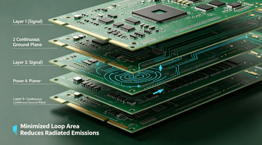
Minimize loop area for LC sections.
Provide a solid ground return path; avoid splitting ground beneath sensitive sections.
For LC filters, avoid long traces from inductor to capacitor (they add inductance and can reduce attenuation).
How To Design A Low Pass Filter That Works
The fastest way to reduce engineering rework and procurement disputes is to define verification deliverables in a table. Below is a practical template you can copy into your internal specification.
| Item to Verify | Method Number + Revision | Sample Plan | Test Conditions | Raw Data Required | Traceability (lot/batch/serial) | Pass/Fail Rule |
|---|---|---|---|---|---|---|
| Cutoff frequency (fc) | HCJM-LPF-RESP-001 Rev.A | n=5 per lot (min), include 1 worst-case location | Source/load fixed; sweep settings documented; 25°C | CSV + response plot | Board serial + build lot | fc within ±X% of target |
| Attenuation at stopband point | HCJM-LPF-RESP-001 Rev.A | Same as above | Same as above | CSV + plot marker | Same as above | ≥ Y dB @ f_stop |
| Passband insertion loss | HCJM-LPF-RESP-001 Rev.A | Same as above | Same as above | CSV + plot | Same as above | ≤ Z dB loss in passband |
| Resonance / peaking (LC) | HCJM-LPF-RESP-002 Rev.A | n=5 per lot | Same + confirm fixture wiring | Plot + notes | Same as above | No peak > P dB above passband |
| Noise/THD (audio) (if required) | HCJM-AUD-TEST-010 Rev.A | n=3 per lot | Define input level, load, bandwidth | FFT plots + levels | Same as above | Meets defined noise/THD limit |
Notes: The method IDs above are examples of a revision-controlled procedure format. The key is that the procedure is versioned and repeatable.
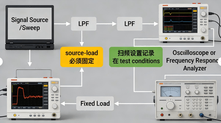
Schematic Diagram Of The Test Bench
Supplier shall verify the low-pass filter frequency response on production units and provide a report including method ID and revision, sample plan, test conditions (source/load, sweep settings, temperature), and raw data (CSV/plots). Traceability must link results to lot/batch/serial identifiers. Acceptance criteria: cutoff frequency within ±X% and attenuation ≥Y dB at specified stopband frequency.
1.Ignoring load impedance: a low pass filter circuit may shift cutoff when connected to a real amplifier or ADC input.
2.Validating high-frequency behavior on a breadboard: parasitics can mask problems or create false confidence.
3.Choosing “steeper order” without stability checks: higher order can create ringing, peaking, or phase issues.
4.LC layout too loose: long traces and poor ground return reduce attenuation and can introduce resonance.
5.No consistent test conditions: changing sweep bandwidth, fixture wiring, or source/load breaks comparability between lots.
A low pass filter on amplifier input or feedback paths can limit bandwidth and reduce high-frequency noise. The practical priority is not only cutoff frequency, but also phase behavior, noise floor, and distortion. Engineers should define measurement bandwidth and input levels so results are repeatable.
An anti-alias low-pass filter prevents high-frequency components from folding into the sampled band. Here, cutoff selection must leave margin below the Nyquist frequency (half the sampling rate). The verification focus is fc accuracy and stable response across component tolerance and temperature.
For switching regulators or PWM-like signals, LPFs are used to attenuate switching harmonics. LC filters can help, but resonance and layout can dominate. Verification should explicitly measure attenuation at switching frequency and key harmonics with fixed fixture conditions.
1) What is a low pass filter in an amplifier?
It is a network that limits high-frequency content in the amplifier signal path, often to reduce noise, prevent oscillations, or shape system bandwidth. The exact effect depends on where it is placed (input, feedback, output) and the amplifier’s impedance and stability margins.
2) How do I pick cutoff frequency for low pass filter audio?
Choose cutoff above the highest desired audio band (or above a target crossover) while ensuring enough attenuation of unwanted high-frequency noise. Then verify phase and group delay if the system is sensitive to timing or transient response.
3) Passive low pass vs active low-pass filter—how to choose?
Use passive RC for low cost and simplicity at low frequencies when loading is controlled. Use active filters when you need stable cutoff under varying load or when you want higher-order response without large inductors. Use LC when you need lower loss at higher power, but plan for resonance control and careful layout.
4) Why does my lowpass filter simulation look correct but hardware doesn’t?
The most common reasons are missing source/load models, ignoring parasitics, and layout effects. Breadboard measurements can also distort results at higher frequencies.
5) What is LPF meaning? Is “lowpass filter” the same thing?
LPF is a common abbreviation for low-pass filter. “Lowpass filter” is an informal spelling; they refer to the same concept.
6) How many stages (order) do I need?
Order depends on how much attenuation you need at a specific frequency. If you require very strong rejection near the passband edge, consider higher order—but validate phase/ringing and tolerance sensitivity.
7) Can I build a low pass filter circuit on a breadboard?
For low-frequency learning and quick checks, yes. For high-frequency or EMI-critical behavior, a PCB prototype is recommended.
1.To reduce procurement risk and make reorders predictable, buyers and engineers can request an evidence pack structured around measurable verification:
2.Revision-controlled test procedure (method number + revision) for LPF response
3.Sample plan document (n per lot, locations, any worst-case selection rule)
4.Test condition sheet (source/load, sweep settings, temperature, fixture notes)
5.Raw data files (CSV) and plotted response curves with markers
6.Instrument model and calibration reference fields (as applicable)
7.Traceability mapping (lot/batch/serial linked to report)
8.Inspection records structure (IQC/IPQC/FQC checkpoints)
9.Reorder consistency notes (what is locked for repeat builds)
10.Change log (what changed between revisions of method/procedure)
11.Packaging/handling notes for sensitive components (if required by the design)
A low-pass filter is simple in concept but easy to misapply in real hardware. The most reliable results come from clear requirements (cutoff, slope, loss, phase), correct topology selection (RC, LC, or active), and a verification plan that locks down source/load conditions and produces raw data that can be audited. When engineering and procurement align on evidence deliverables—method number + revision, sample plan, test conditions, raw data, and traceability—projects move faster and scale more safely.
Quick Answer: What is the NPI Process? The NPI process (New Product Introduction) is the engineering
Explore the PCB Manufacturing Process from design and imaging to etching, drilling, plating, and fin
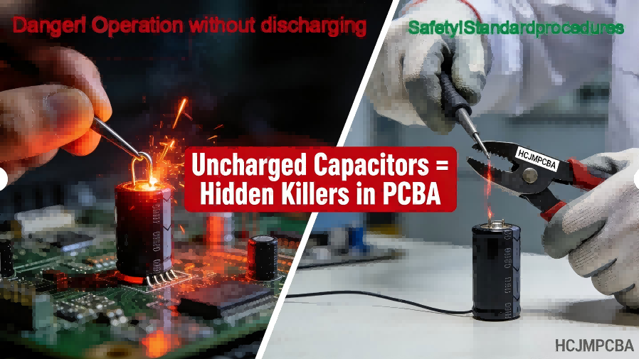
Discharging capacitors is a critical safety and quality control step in electronics and PCBA work. T