How to Produce Multilayer Circuit Board: 12 Precise Steps for Complex Electronics
Discover the end-to-end process to produce a multilayer circuit board, from stack‑up planning and
An hdi pcb (High Density Interconnect PCB) is a type of high density circuit board that uses microvias, fine lines (<75µm), and advanced layer interconnect structures such as blind and buried vias to achieve higher wiring density. This guide is maintained by the HCJMPCBA engineering team and updated with production-grade checklists to ensure manufacturability and reliability in mass production.
The evolution of high density interconnect pcb design is driven by increasing component density, especially for fine-pitch BGA packages.
Typical structures include:
1+N+1 HDI: One build-up layer on each side of a core
2+N+2 HDI: More routing flexibility for complex designs
ELIC PCB (Every Layer Interconnect): Full interconnect between all layers
Sequential lamination is the core process enabling these structures. Each lamination cycle must be tightly controlled to avoid delamination and misalignment.

Hcjmpcba Cross Section Of Hdi Versus Ordinary Pcb
| Parameter | Standard PCB | HDI PCB |
|---|---|---|
| Pitch | >0.65mm | <0.5mm |
| Via Size | >0.2mm | 0.075–0.15mm |
| Line Width | >100µm | <75µm |
| Density | Medium | High |
| Cost | Lower | Higher per unit but lower system cost |
Conclusion:
When design density, signal speed, or space constraints increase, transitioning to high density interconnect pcbs becomes unavoidable.
Choose appropriate IPC-2226 classification (Type I/II/III).
This determines via structure and stacking complexity.
High-performance hdi multilayer pcb requires:
High Tg materials
Low Dk/Df laminates
Controlled thermal expansion
Typical ratio:
Depth : Diameter ≤ 1:1
Improper ratio leads to:
plating voids
early failure
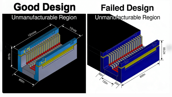
Hcjmpcba Microvia Aspect Ratio Diagram
Fine-pitch bga pcb requires:
via-in-pad
dog-bone routing
Controlled impedance
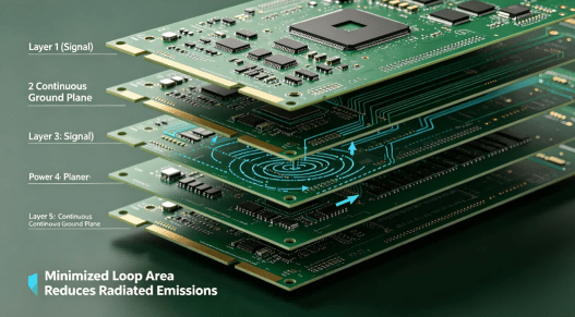
Reference plane stability
Crosstalk reduction
At HCJMPCBA, DFM is not optional:
Each project is assigned:
Method Number
Revision Control
This ensures consistent production behavior.
Mass production of hdi pcbs is where most suppliers fail.
At HCJMPCBA:
Each process = defined Method Number
Each change = tracked via Revision
We implement:
AQL-based Sample Plan
Controlled Test Conditions (Temp/Humidity)
Testing includes:
Thermal cycling
IST (Interconnect Stress Test)
Every hdi pcb board is linked to:
Lot number
Batch number
Serial number
We provide:
AOI raw data
Laser drilling logs
Electrical test reports

Hcjmpcba Screenshot Of Pcb Traceability Report
| Metric | Industry | HCJMPCBA |
|---|---|---|
| Drill Accuracy | ±25µm | ±10µm |
| Lamination | Manual | PLC Controlled |
| Cross-section | Random | Sample Plan |
| Microvia Test | Visual | 4-wire testing |
The supplier shall manufacture hdi printed circuit boards per IPC-6012 Class 3. All microvias must comply with IPC-4761 Type VII. The supplier must provide raw data, and full traceability (lot/batch/serial) linked to method number and revision control.
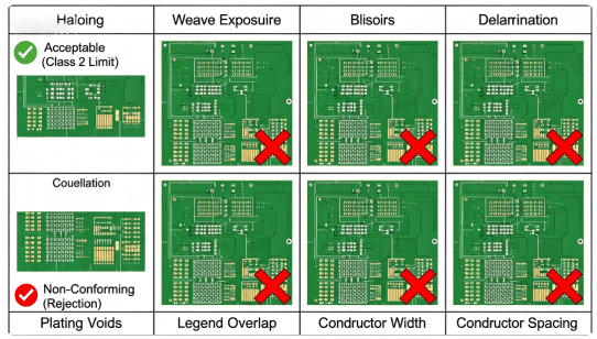
1.Ignoring microvia aspect ratio
2.Overusing stacked vias
3.Wrong material selection
4.Poor BGA fan-out
5.Uneven copper distribution
A client transitioned:
From 12-layer standard PCB
To 8-layer elic pcb
Result:
Reduced size
Improved signal integrity
Lower system cost
Q1: What is HDI PCB?
A high-density interconnect board using microvias and fine routing.
Q2: What is the typical HDI PCB price?
Higher per unit, but reduces overall system cost.
Q3: How to ensure microvia reliability?
Through controlled test conditions and IST testing.
Q4: What standards apply?
IPC-2226 and IPC-6012.
Q5: Can HCJMPCBA produce ELIC PCB?
Yes, with full process control.
Q6: What is minimum trace width?
Down to 50µm depending on design.
Microsection reports
Reflow profiles
X-ray inspection data
Raw electrical testing data
Designing and manufacturing a reliable hdi pcb is not just about density—it is about control, data, and repeatability.
At HCJMPCBA, we transform complex hdi design into scalable mass production through:
Methodized process control
Verified test conditions
Full traceability
For more information about PCBA services, please contact Guangzhou Huachuang Precision Technology(HCJMPCBA).
Update triggers: standard revision changes / recurring questions / production checklist updates.
Discover the end-to-end process to produce a multilayer circuit board, from stack‑up planning and
Discover what does PCB stand for in this comprehensive guide by HCJMPCBA. Learn about ict tester rol
1. The Physics Behind PCB Shielding: Reflection, Absorption, and Grounding To deploy an effective bo