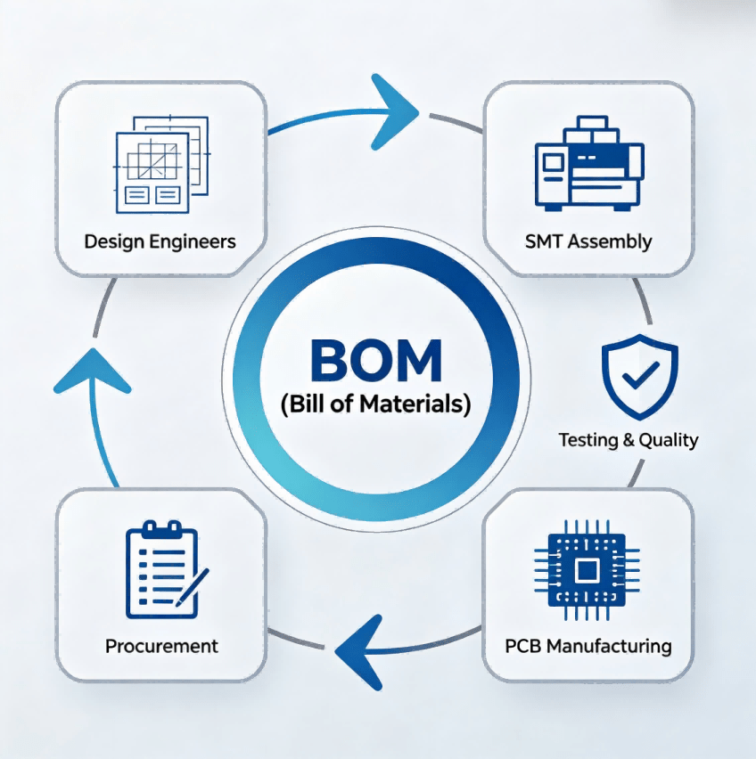
15 Practical Insights Into Relays: What Does a Relay Do & How It Works in PCBA Design
This comprehensive guide explains relays, what a relay does, and how relays work in electronic and P
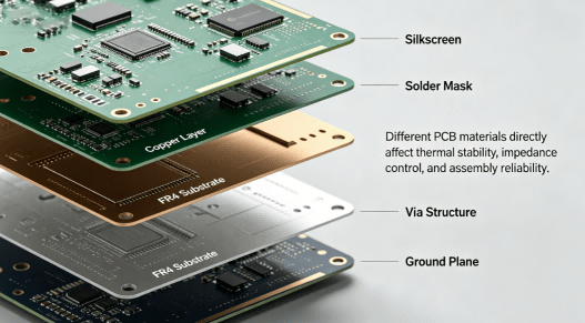
Modern pcb circuit boards are primarily made of fiberglass-reinforced epoxy laminates (FR-4), copper foil, resin systems, solder mask coatings, and printed silkscreen markings. These materials work together to provide electrical conductivity, insulation, heat resistance, and mechanical stability.
The manufacturing process typically includes imaging, etching, drilling, copper plating, solder mask application, surface finishing, electrical testing, and PCB assembly. Material selection and process control directly affect long-term reliability, solderability, thermal stability, and manufacturing yield.
This guide is maintained by the HCJMPCBA engineering team and updated with production checklists.
1. PCB Reliability Starts with Material Selection
The thermal stability, dielectric behavior, and copper structure of a board determine whether a PCB can survive reflow soldering, vibration, and long-term field operation.
2. Manufacturing Consistency Depends on Process Control
Copper etching accuracy, hole wall quality, solder mask alignment, and layer lamination directly influence final circuit card assemblies yield.
3. Traceability Is Becoming a Core Manufacturing Requirement
Modern PCBA production increasingly relies on revision control, lot tracking, raw inspection data, and serial-based traceability to reduce supply chain risk.
Many people searching for terms like “what are circuit boards made of” or “what are pcbs made of” assume that a PCB is simply a thin plastic board with copper traces. In reality, modern printed circuit board materials are carefully engineered combinations of conductive metals, insulating substrates, chemical coatings, and thermal management structures.
Each layer inside a PCB serves a specific electrical or mechanical purpose.
FR-4 is the most widely used printed circuit board material in the electronics industry.
It consists of woven fiberglass cloth impregnated with epoxy resin. The fiberglass provides structural rigidity, while the resin offers insulation and thermal resistance.
FR-4 became the industry standard because it balances:
Different FR-4 grades exist depending on thermal requirements. High-Tg FR-4 materials are commonly used in industrial control systems, automotive electronics, and multilayer boards exposed to repeated thermal cycling.
When engineers ask:
“What is a PCB made of?”
FR-4 is usually the foundation of the answer.
Copper is the conductive backbone of every pcb circuit.
Thin copper foil layers are laminated onto the substrate and later etched into traces, pads, planes, and vias. These conductive pathways allow electrical signals and power to travel between components.
Copper thickness directly affects:
Typical copper weights include:
Applications such as motor drives, industrial robotics, and automotive power systems often require thicker copper structures to handle high current loads.
The resin system inside a PCB affects both electrical and thermal performance.
Common resin systems include:
Important properties include:
Poor resin selection can lead to:
This is one reason why high-speed and automotive electronics require stricter material validation.
The solder mask is the colored protective coating applied over exposed copper.
Most solder masks are green, although black, white, blue, and red variants are also common.
Solder mask functions include:
Without solder mask protection, copper surfaces would oxidize quickly and become difficult to solder reliably.
Silkscreen is the printed legend layer used for identification and assembly reference.
Typical silkscreen information includes:
Although silkscreen does not directly affect electrical performance, it significantly improves assembly efficiency and maintenance clarity.
A pcb circuit is a network of conductive copper pathways built onto an insulating substrate to electrically connect electronic components.
Unlike point-to-point wiring, PCB structures provide:
However, not all PC boards behave the same way.
Material selection directly influences:
For example:
A low-cost FR-4 board may function perfectly in a consumer toy but fail rapidly inside an industrial motor controller exposed to high temperatures and vibration.
This is why printed circuit board materials must always match the electrical and environmental demands of the final product.
| Material | Typical Use | Advantages | Limitations |
|---|---|---|---|
| Standard FR-4 | Consumer Electronics | Cost-effective | Moderate thermal resistance |
| High-Tg FR-4 | Industrial & Automotive | Better thermal stability | Higher cost |
| Polyimide | Aerospace & Military | Excellent heat resistance | Expensive |
| Aluminum PCB | LED & Power Systems | Superior heat dissipation | Limited routing flexibility |
| Rogers High-Frequency Material | RF & Microwave | Low signal loss | Higher fabrication cost |
Hcjmpcba Layered Section View Of Pcb Materials
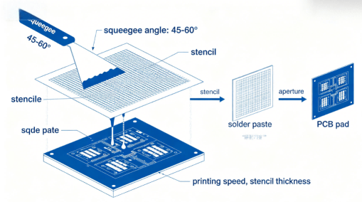
PCB manufacturing begins with copper-clad laminate preparation.
Large production panels are cut into manufacturing sizes according to the product stack-up and process requirements.
At this stage, manufacturers verify:
Improper material storage can introduce moisture absorption, which later causes delamination during soldering.
For multilayer boards, the internal copper layers must first be patterned.
A photoresist film is laminated onto the copper surface, then exposed using UV imaging equipment.
The exposed areas define the future circuit layout.
This stage determines:
Poor imaging alignment can later create impedance instability and short circuits.
After imaging, unwanted copper is chemically removed.
Only the protected copper remains, forming the actual electrical circuitry.
Etching precision is critical because excessive copper removal can create:
Modern PCB fabrication lines continuously monitor etching chemistry and conveyor speed to maintain process consistency.
Multilayer PCB structures are created by stacking:
These layers are pressed together under controlled temperature and pressure.
Proper lamination prevents:
As board layer counts increase, stack-up symmetry becomes increasingly important.
CNC drilling machines create:
After drilling, the hole walls are chemically plated with copper to establish electrical conductivity between layers.
Hole wall quality strongly affects long-term reliability.
Poor metallization may cause intermittent electrical failures after thermal cycling.
The solder mask coating is applied over exposed copper except for pads intended for soldering.
This stage improves:
Precise solder mask alignment is particularly important for fine-pitch SMT components.
PCB surface finishes protect exposed copper before assembly.
Common finishes include:
Surface finish selection affects:
ENIG is widely used for high-density PCBA because of its flat surface and oxidation resistance.
Before shipment, fabricated PCBs undergo electrical verification.
Testing methods may include:
This stage confirms circuit continuity and detects open or short circuits before assembly begins.
Bare boards become functional products during PCBA assembly.
Typical assembly stages include:
Assembly quality ultimately depends on both PCB fabrication quality and component process control.
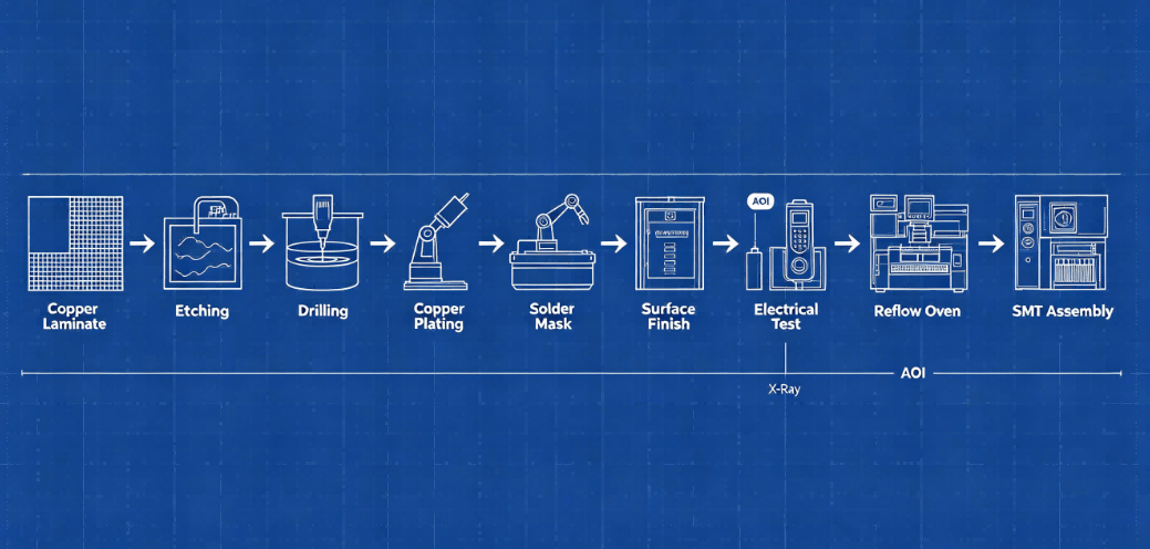
Hcjmpcba Pcb Manufacturing Process Flow
PCB materials influence much more than mechanical support.
Electrical performance is heavily affected by:
For example:
High-speed communication boards require stable dielectric properties to maintain impedance consistency.
Power electronics require thicker copper and stronger thermal dissipation structures.
Automotive and industrial systems often require high-Tg materials to survive repeated thermal cycling.
Improper material selection may create:
At Guangzhou Huachuang Precision Technology (HCJMPCBA), manufacturing consistency is managed through revision-controlled production systems.
Engineering teams maintain:
This helps prevent uncontrolled process variation between prototype and production batches.
Inspection strategies are selected according to:
Typical verification methods include:
Sample plans follow defined acceptance methodologies depending on risk level and production volume.
Modern OEM customers increasingly request production evidence beyond simple pass/fail reports.
Typical retained records include:
Traceability structures support faster root-cause analysis if reliability concerns emerge later.
| Verification Item | Typical Standard |
|---|---|
| Copper Thickness | IPC-6012 |
| Hole Wall Integrity | IPC-TM-650 |
| Solder Mask Alignment | IPC-SM-840 |
| Surface Finish Thickness | Customer Specification |
| Electrical Continuity | 100% Test |
| Traceability Records | Internal Control |
| Thermal Profile Archive | Process Controlled |
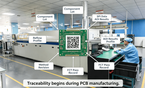
Hcjmpcba Traceability System Diagram
1. Using Standard FR-4 in High-Temperature Applications
Low-Tg materials may fail under repeated thermal cycling.
2. Ignoring Copper Balance
Uneven copper distribution often causes warpage during reflow soldering.
3. Selecting the Wrong Surface Finish
Some finishes are unsuitable for fine-pitch or high-reliability assemblies.
4. Underestimating Moisture Absorption
Improper storage conditions can damage PCB laminates before assembly even begins.
5. Poor Stack-Up Planning
Unbalanced multilayer structures increase stress and reduce long-term reliability.
An industrial motor controller project originally experienced repeated solder cracking and PCB warpage during thermal cycling tests.
Investigation revealed several issues:
After redesigning the stack-up using high-Tg FR-4 and optimized copper distribution, the updated board achieved significantly improved assembly consistency and thermal reliability during production testing.
This example demonstrates how PCB material decisions directly affect downstream PCBA stability.
Supplier shall maintain revision-controlled fabrication records, material traceability documentation, electrical test reports, and process verification archives for all PCB and PCBA production lots.
What are printed circuit boards made of?
Most PCBs are made from fiberglass-reinforced epoxy laminates (FR-4), copper foil, solder mask coatings, and printed silkscreen markings.
What is FR-4 material?
FR-4 is a fiberglass-reinforced epoxy laminate commonly used as the insulating base material in PCBs.
Why is copper used in PCB circuits?
Copper provides excellent electrical conductivity and can be precisely etched into signal traces and power structures.
How are multilayer PCBs manufactured?
Multiple etched copper layers are laminated together under heat and pressure, then drilled and plated to create interconnections.
What is solder mask used for?
Solder mask protects copper traces from oxidation and helps prevent accidental solder bridging during assembly.
What surface finish is best for PCBA?
The best finish depends on the application. ENIG is commonly used for high-density SMT assemblies because of its flatness and oxidation resistance.
Why does PCB material affect thermal reliability?
Different materials expand differently under heat. Poor thermal compatibility can lead to cracking, warpage, or delamination.
How do PCB manufacturers verify board quality?
Manufacturers typically use AOI, electrical testing, impedance verification, and process inspection systems to verify PCB quality.
Engineering teams may request:
These records help validate process consistency and manufacturing control capability.
Modern pcb circuit boards are highly engineered structures made from conductive copper layers, insulating laminates, protective coatings, and precision fabrication processes. Material selection and manufacturing control directly influence thermal reliability, electrical stability, assembly yield, and long-term product performance.
As electronics continue moving toward higher density, higher speed, and higher reliability requirements, understanding how printed circuit boards are made becomes increasingly important for both engineering and procurement teams.
Update triggers: standard revision changes / recurring questions / production checklist updates.
This comprehensive guide explains relays, what a relay does, and how relays work in electronic and P
Discover what a 10k resistor is, how to read its color bands, and why this fundamental component is
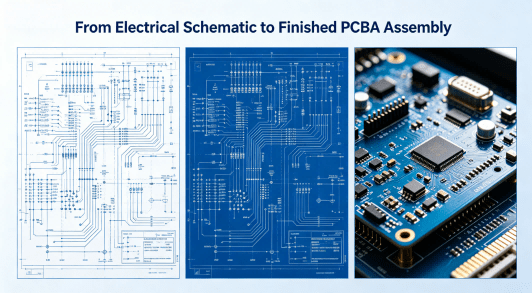
Learn what an electrical schematic is, how to read a circuit diagram, and how PCB/PCBA manufacturing