Engineering Reliability: The Ultimate Guide to PCBA Quality Assurance | HCJMPCBA
Learn how HCJMPCBA ensures zero-defect PCBA through ISO 13485 compliance, IPC Class 3 standards, 3D
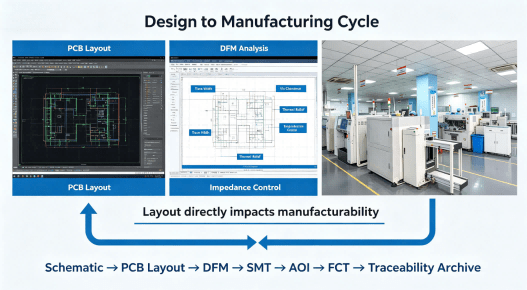
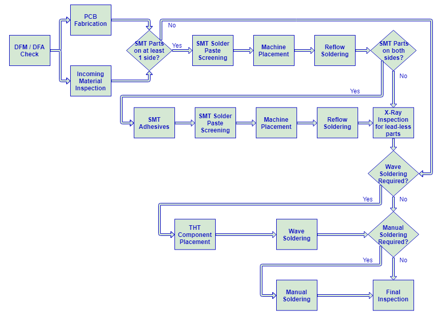
Professional pcb design services are required whenever a product moves beyond experimental wiring into manufacturable electronics. From startups building IoT hardware to automotive electronics teams and industrial control integrators, reliable PCB layout directly affects signal integrity, thermal stability, EMI behavior, assembly yield, and long-term field reliability. Proper layout is not only about connecting circuits — it determines whether a board can survive automated PCB assembly, reflow stress, vibration, and large-scale production.
This guide is maintained by the HCJMPCBA engineering team and updated with production checklists to ensure design files comply with international assembly standards.
More than 70% of assembly-related defects originate from poor layout decisions rather than SMT machine capability. Trace spacing, thermal balancing, and footprint accuracy directly affect circuit card assemblies during mass production.
Modern products require layout planning that considers automated assembly, solderability, thermal behavior, testability, and future revision management before Gerber release.
Embedding serial tracking zones, revision control structures, and inspection access points during PCB layout reduces supply chain failures and simplifies lifecycle management.
Many companies assume PCB layout is simply “drawing traces.” In reality, layout engineering sits between electrical theory and physical manufacturing constraints.
A schematic may function electrically, but without proper layout optimization, the final PCB can suffer from:
This is why professional printed circuit board design services have become increasingly important across industries.
Startups developing robotics, IoT systems, embedded AI modules, guitar pedal pcb systems, industrial gateways, or wearable devices often begin with functional prototypes. However, transitioning from a working prototype into scalable manufacturing requires specialized pcb layout services.
Teams searching for terms such as:
are often facing the same challenge:
“The prototype works, but it is not manufacturable at scale.”
Typical risks include:
Professional layout review eliminates these issues before the first production run.
High-reliability sectors require significantly tighter PCB layout control.
Applications such as:
must comply with stricter thermal, vibration, and electrical reliability requirements.
In these environments, pcb manufacturers in china are often selected not only for assembly capability, but for their ability to participate in layout optimization and DFM verification.
Many engineering teams sourcing through local directories or independent design hubs eventually encounter manufacturing inconsistencies during low-volume production.
Common problems include:
This is where integrated circuit board layout services become valuable because layout decisions directly affect SMT efficiency and inspection quality.
| Capability | Internal Design Team | Freelance Contractor | DFM-Integrated EMS Partner |
|---|---|---|---|
| Manufacturing Awareness | Medium | Low | High |
| Assembly Optimization | Limited | Variable | Integrated |
| DFM Review | Optional | Rare | Standardized |
| Signal Integrity Validation | Depends on Experience | Limited | Structured |
| Traceability Planning | Rare | Rare | Embedded |
| Revision Management | Internal Only | Fragmented | Controlled |
| Transition to Mass Production | Difficult | Risky | Streamlined |
| Raw Manufacturing Feedback | Minimal | None | Continuous |
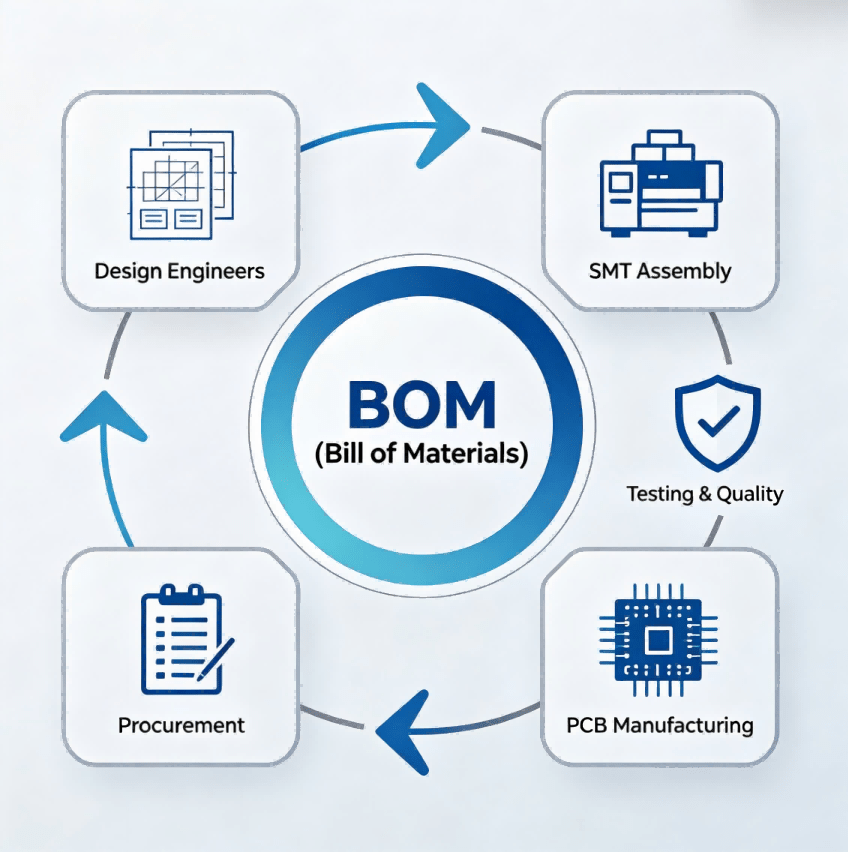
Engineering teams increasingly prefer integrated EMS-oriented pcb design company workflows because manufacturing feedback is incorporated before production begins.
Hcjmpcba Closed Loop Diagram From Design To Mass Production
Every PCB begins with electrical logic.
At this stage, engineers define:
Accurate netlist generation is essential because every downstream layout process depends on electrical connectivity integrity.
Proper layer planning affects:
Most multilayer designs follow IPC-2221 recommendations for spacing, isolation, and routing structures.
Typical stack-up considerations include:
Poor stack-up planning is one of the leading causes of rework during PCB prototype validation.
Placement determines assembly efficiency and thermal behavior.
Critical placement principles include:
In automated pcb assembly environments, improper spacing often creates hidden inspection zones that increase escape risk.
Routing is not simply drawing copper connections.
High-speed designs require:
Professional pcb layout design services typically use simulation tools to validate critical signal behavior before Gerber release.
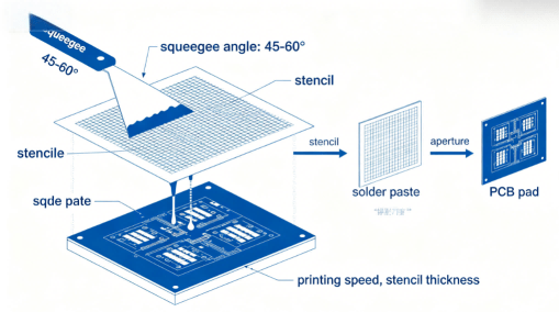
Uneven copper distribution creates thermal stress during reflow.
Common consequences include:
Balanced copper structures help stabilize thermal expansion across the board.
Before production release, SI and PI analysis validates:
Verification reduces expensive redesign cycles later in manufacturing.
Final production files typically include:
Missing or inconsistent documentation remains a major source of production delays.
At Guangzhou Huachuang Precision Technology (HCJMPCBA), layout manufacturability review is integrated into the transition between engineering prototypes and scalable PCBA production.
Instead of treating layout and assembly as separate departments, engineering teams evaluate how layout decisions affect:
Revision consistency becomes increasingly important during iterative hardware development.
HCJMPCBA maintains:
This helps prevent uncontrolled production drift between prototype and batch manufacturing stages.
Inspection strategies are adapted according to:
Typical inspection methods include:
Sample plans follow defined AQL methodologies depending on production volume and risk level.
Modern OEM customers increasingly request actual production evidence rather than summary reports.
Typical retained records include:
Raw data retention supports root-cause analysis and long-term traceability.
Traceability structures may include:
This enables rapid containment if component reliability issues emerge later in the product lifecycle.
| Verification Item | Typical Requirement |
|---|---|
| Trace Width & Clearance | IPC-2221 compliant |
| Footprint Accuracy | IPC-7351 aligned |
| Thermal Relief Design | Verified |
| AOI Accessibility | Confirmed |
| Copper Balance | Reviewed |
| Solder Mask Clearance | Verified |
| Test Point Accessibility | Included |
| Revision Identification | Controlled |
| Manufacturing Notes | Complete |
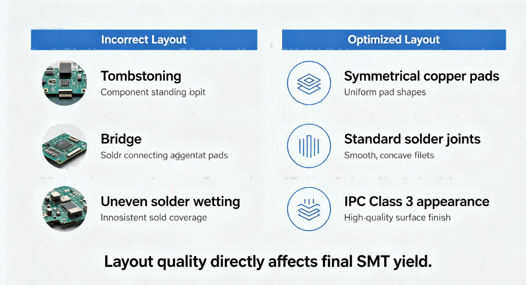
Hcjmpcba Defect Comparison Caused By Poor Layout
1. Incorrect Footprint Dimensions
Ignoring IPC-7351 standards creates assembly alignment issues and unreliable solder joints.
2. Poor Thermal Relief Structures
Excessive copper connection without proper thermal relief causes cold soldering during reflow.
3. Inadequate Clearance for High-Speed Circuits
Tight spacing increases crosstalk and EMI instability.
4. Copper Imbalance
Asymmetrical copper distribution causes board bending during thermal cycling.
5. Missing Manufacturing Documentation
Incomplete drill tables or unclear assembly notes create avoidable engineering delays.
An automotive controller project initially began as a low-volume prototype using standard pcb layout services.
The first revision experienced:
After DFM review, engineers modified:
The updated revision passed thermal cycling and successfully transitioned into higher-volume automated PCB assembly.
This type of transition highlights why manufacturing-aware PCB layout is increasingly important in modern electronics development.
What is the difference between schematic design and PCB layout?
A schematic defines electrical logic, while PCB layout defines the physical implementation required for manufacturing and assembly.
Why is PCB layout important for mass production?
Layout affects solderability, inspection access, thermal behavior, and assembly yield during automated manufacturing.
What standards are commonly used in PCB layout?
Common standards include IPC-2221, IPC-7351, IPC-A-610, and J-STD-001.
Can poor layout increase PCB assembly cost?
Yes. Poor layouts often increase rework rates, reduce SMT efficiency, and create manufacturing delays.
Why are thermal vias important?
Thermal vias help transfer heat away from high-power components and improve thermal reliability.
What files are required for PCB manufacturing?
Typical files include Gerber, BOM, centroid data, fabrication drawings, and assembly notes.
Why is traceability important in PCBA?
Traceability enables faster root-cause analysis and controlled containment if reliability issues occur.
Evidence You Can Request During Factory Audits
Many EMS-oriented PCB manufacturers provide DFM feedback before production release.
Evidence You Can Request During Factory Audits
Engineering teams may request:
These records help validate manufacturing process consistency.
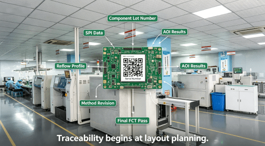
Hcjmpcba Traceability System
Professional pcb design services are no longer limited to drawing traces between components. Modern PCB layout directly affects manufacturability, reliability, inspection efficiency, thermal behavior, and long-term field stability.
As electronic systems become more complex, engineering teams increasingly require layout workflows that integrate DFM validation, inspection planning, revision control, and scalable manufacturing readiness from the earliest design stages.
Update triggers: standard revision changes / recurring questions / production checklist updates.
Learn how HCJMPCBA ensures zero-defect PCBA through ISO 13485 compliance, IPC Class 3 standards, 3D
Explore the comprehensive guide to industrial pcb production and the professional pcb manufacturing
A low pass filter is a circuit that allows low-frequency signals to pass while attenuating higher-fr