12 Critical Insights into Series Circuits: The Industrial Engineer’s Guide to High-Reliability PCBA Manufacturing
Looking for a definitive guide on what is a series circuit? This engineering deep dive by the HCJMPC
Common PCB Issues and Repairs: A Practical Guide for Engineers and Procurement Teams
Table of Contents
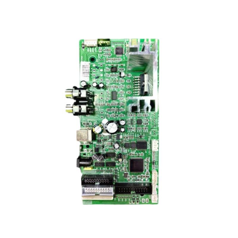
TogglePrinted circuit boards (PCBs) are the structural and electrical backbone of virtually every electronic device — from industrial control systems and medical equipment to consumer electronics and automotive modules. They provide mechanical support and electrical interconnections that enable components to work together as a functioning system.
Despite advances in materials and manufacturing processes, PCBs remain susceptible to various faults that can cause device malfunction or complete failure. For hardware engineers and procurement teams, understanding these failure modes — and how to prevent them — is essential for ensuring product reliability and minimizing costly downtime.
At Guangzhou Huachuang Precision Technology Co., Ltd. (HCJMPCBA), we approach PCB quality as a process discipline, not an inspection outcome. With nearly 3,500 m² of ESD‑protected manufacturing space, multiple high-speed SMT lines, and ISO9001 quality management and ISO13485 medical device quality management certifications, we build reliability into every board we manufacture. The best PCB repair is the one that never becomes necessary — and that starts with robust manufacturing processes.
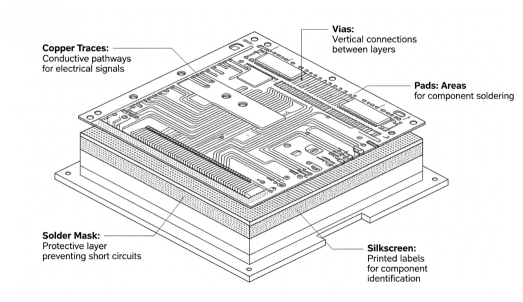
Pcb Structure Diagram
Physical damage is the most visible form of PCB failure. It typically results from mechanical stress — drops, impacts, rough handling, or excessive force during assembly or installation. This stress can cause:
Substrate cracks — Fractures in the board material that can sever internal connections
Broken traces — Copper paths physically severed, interrupting electrical continuity
Lifted pads — Copper pads detached from the substrate, making component soldering impossible
Damaged connectors — Bent or broken pins that prevent proper mating
Physical damage is usually identifiable through visual inspection. Look for:
Visible cracks or fractures on the board surface
Copper traces that appear broken or scratched
Pads that are lifted or no longer flush with the board surface
Bent or missing connector pins
Repairing physical damage typically requires precision work by trained technicians with appropriate equipment:
Broken traces — Can be repaired by soldering a fine wire bridge across the break, or by applying conductive ink to re-establish the circuit path
Lifted pads — May require epoxy adhesive to reattach the pad, followed by careful soldering
Cracked substrates — Often irreparable; the board may need replacement if cracks extend through multiple layers
Prevention is more effective than repair. Proper handling procedures, ESD-safe packaging, and mechanical design that accounts for real-world stresses all reduce the risk of physical damage.
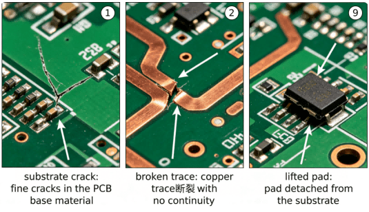
Diagram Of Physical Damage Types
Components themselves can fail due to aging, thermal stress, electrical overload, or voltage surges. Common culprits include:
Capacitors — Electrolytic capacitors are particularly prone to drying out, bulging, or leaking
Resistors — Can drift out of tolerance or fail open due to overcurrent
Diodes and transistors — May fail short or open due to voltage spikes
Integrated circuits — Can be damaged by ESD, overvoltage, or thermal stress
Diagnosing component failure typically involves:
Visual inspection — Look for bulging capacitors, burn marks, discoloration, or cracked packages
Multimeter testing — Check for opens, shorts, and incorrect resistance or capacitance values
Oscilloscope analysis — Verify signal waveforms at critical nodes
Thermal imaging — Identify components running abnormally hot
Repair involves desoldering the failed component and replacing it with an identical or electrically equivalent part. Compatibility is critical — using a substitute with different specifications can cause repeated failure.
Prevention requires:
Proper component derating — operating components well below their maximum ratings
Adequate thermal management — ensuring heat-generating components have sufficient cooling
ESD protection during handling and assembly
Using components from reputable suppliers with full traceability
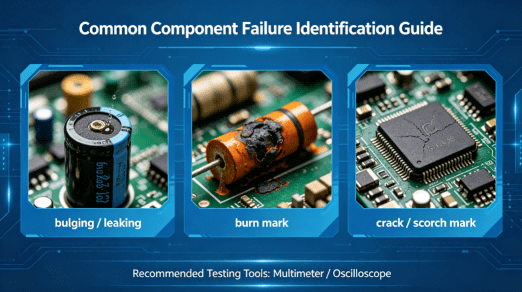
Component Fault Identification Guide Diagram
PCB traces are the copper pathways that carry electrical signals and power between components. Traces can become damaged through:
Mechanical wear — Scratches from handling or contact with sharp objects
Corrosion — Exposure to moisture, chemicals, or contaminants
Electrical overstress — Excessive current causing the trace to act as a fuse and melt
Manufacturing defects — Under-etching, nicks, or incomplete plating
Trace damage can cause complete or partial circuit failure, leading to intermittent faults that are notoriously difficult to diagnose.
Visual inspection — Look for visible breaks, scratches, or discoloration
Continuity testing — Use a multimeter to check for open circuits between trace endpoints
Microscopic inspection — For fine-pitch traces, magnification may be required
Repair methods include:
Wire bridging — Soldering a fine insulated wire across the broken section
Conductive ink — Applying conductive epoxy or ink to bridge the gap
Trace replacement — Soldering a new copper trace over the damaged area
Prevention focuses on manufacturing quality:
Proper etching and plating processes to ensure trace integrity
Adequate trace width for expected current levels
Conformal coating to protect against corrosion and moisture
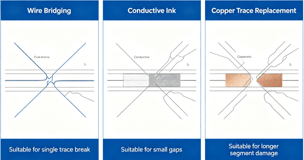
Comparison Of Methods For Repairing Damaged Wiring
Plated through-holes (PTHs) provide electrical connections between different layers of a multilayer PCB. Plating gaps occur when the electroplating process fails to deposit copper completely within the hole, resulting in an incomplete or absent connection between layers.
This defect can be caused by:
Process contamination — Residue or debris in the hole preventing plating adhesion
Inadequate agitation — Poor solution flow during electroplating
Drilling defects — Rough hole walls that prevent uniform plating
X-ray inspection — Reveals incomplete plating within the hole
Resistance measurement — Higher-than-expected resistance between layers indicates a partial connection
Cross-sectioning — Destructive analysis that shows the plating profile
Repair typically involves re-drilling the through-hole and re-plating it with copper. This is a delicate process requiring precise control of the electroplating parameters.
Prevention is far more effective:
Strict quality control during the drilling and plating processes
Regular maintenance of plating solutions and equipment
Inspection of plating quality on a sample basis
Using experienced PCB manufacturers with proven process controls
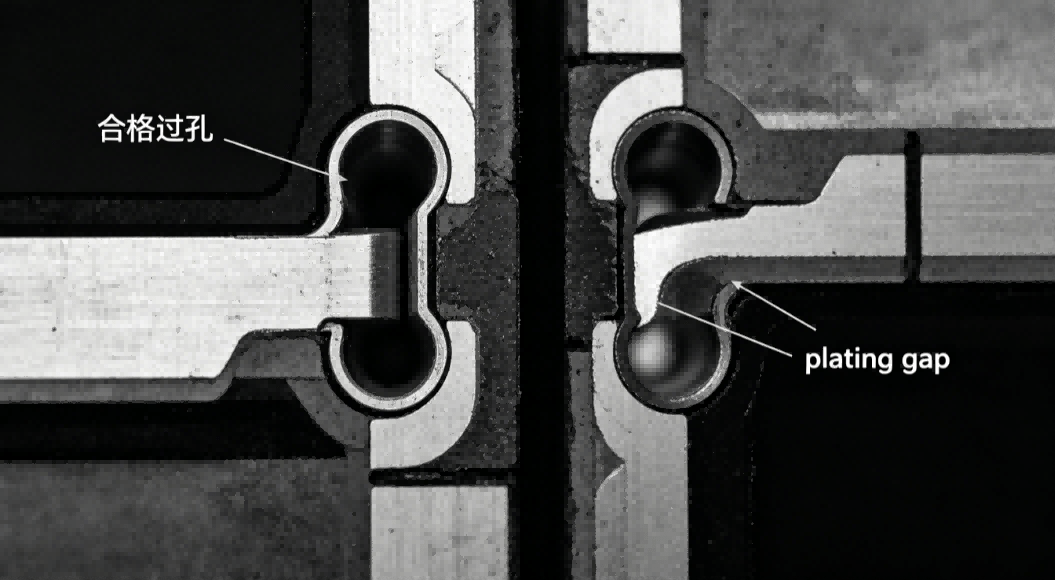
Schematic Diagram Of Through Hole Coating Defects
Power supply failures occur when the board’s power distribution network cannot deliver stable, adequate power to all components. Common causes include:
Faulty power supply components — Failed voltage regulators, diodes, or capacitors
Short circuits — Unintended connections between power and ground
Overloading — Components drawing more current than the supply can deliver
Poor PCB design — Inadequate trace widths for power distribution
Diagnosing power failures requires:
Voltage measurement — Check that supply voltages are within specification at each power rail
Current measurement — Verify that total current draw is within expected limits
Thermal imaging — Identify hot spots that indicate short circuits or overloaded components
Repair may involve:
Replacing failed power supply components
Reseating loose connectors
Repairing short circuits
Reinforcing the power distribution network
Prevention requires:
Proper power supply design with adequate headroom
Sufficient trace widths for power distribution
Adequate decoupling capacitance near each IC
Overcurrent protection where appropriate
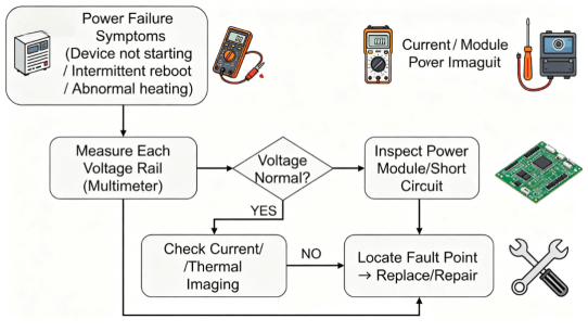
Power Fault Diagnosis Flowchart
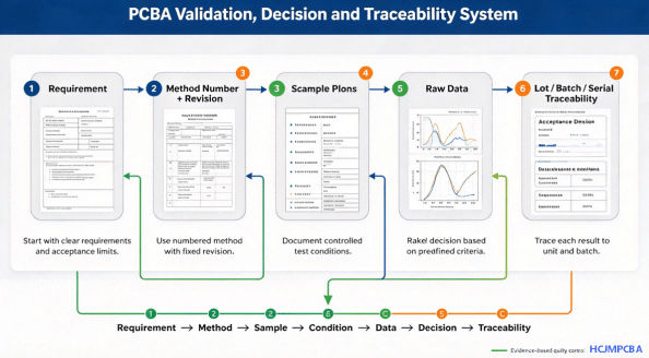
The most effective way to address PCB issues is to prevent them from occurring in the first place. This requires a manufacturing partner with disciplined processes, comprehensive inspection, and full traceability.
At HCJMPCBA, our approach to PCB quality includes:
Comprehensive Inspection — 3D SPI for solder paste verification, AOI after reflow, X-ray for BGA and via inspection, and ICT/functional testing for electrical validation. We catch defects before they become field failures.
Process Control — Statistical process control (SPC) monitoring of key parameters — paste volume, reflow temperature, placement accuracy — with corrective action triggered before defects occur.
Material Traceability — Every component and material lot is tracked through our MES system, providing complete history from receipt to shipment.
Quality Certifications — ISO9001 and ISO13485 quality management systems provide the framework for consistent, documented processes across all production stages.
Scalable Production — From prototype runs of a few boards to mass production of tens of thousands per month, with consistent quality standards across all volumes.
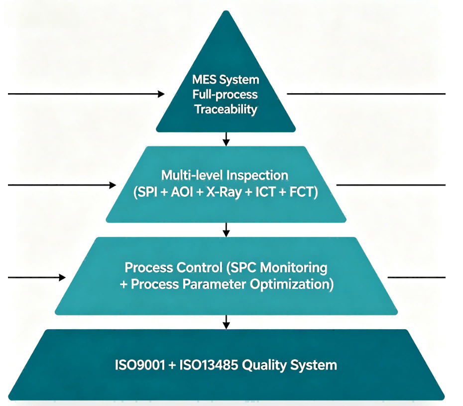
Pcb Quality Problem Prevention System Diagram
Not every PCB issue is worth repairing. Engineers and procurement teams should consider:
Repair is appropriate when:
The damage is localized and repairable (e.g., a single broken trace or failed component)
The board is expensive, difficult to replace, or part of a larger assembly
The board is in a prototype or low-volume production phase
Replacement is more cost-effective when:
The damage is extensive (e.g., multiple layers cracked or widespread component failure)
The board is relatively low-cost compared to the labor cost of repair
Reliability is critical and the board has a history of failures
The board has reached the end of its expected service life
For high-reliability applications — medical devices, industrial controls, automotive systems — replacement is often the safer choice. The cost of a field failure far exceeds the cost of a new board.
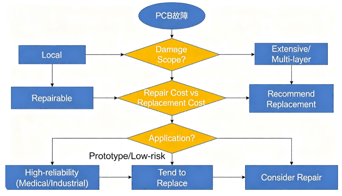
Repair And Replacement Decision Flowchart
PCB issues — physical damage, component failure, trace damage, plating gaps, and power failures — are inevitable in electronics manufacturing. But how they are handled makes the difference between a minor production delay and a major field failure.
For hardware engineers, understanding these failure modes enables better design decisions and more effective troubleshooting. For procurement teams, choosing a manufacturing partner with robust quality systems and process controls reduces the likelihood of these issues reaching production.
At Guangzhou Huachuang Precision Technology Co., Ltd. (HCJMPCBA), we build quality into every board from the start. Our nearly 3,500 m² ESD‑protected facility, multiple high-speed SMT lines, and ISO9001 and ISO13485 certifications provide the foundation for reliable PCB manufacturing — because the best repair is the one you never need.
Looking for a definitive guide on what is a series circuit? This engineering deep dive by the HCJMPC
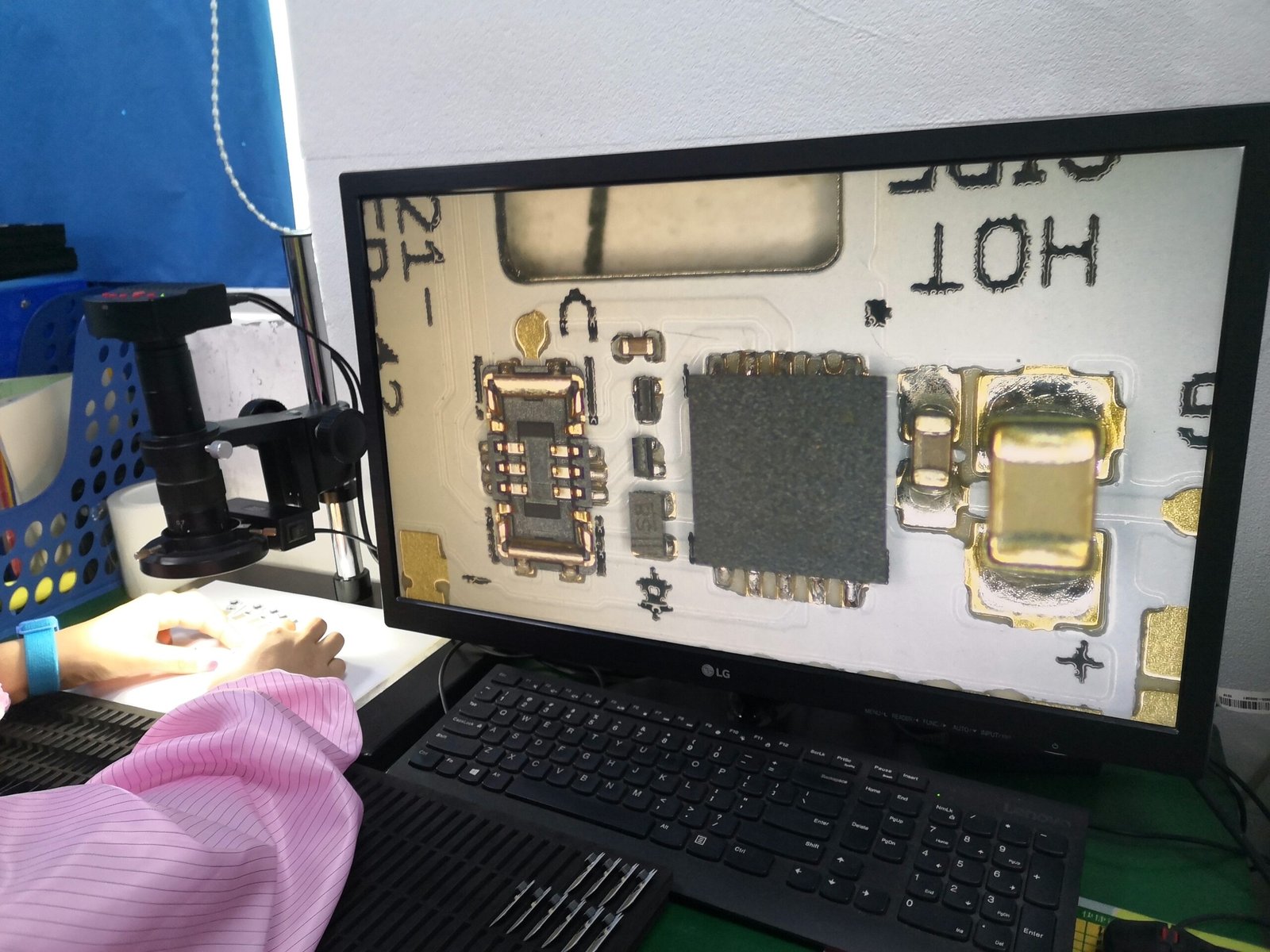
Guangzhou Huachuang Precision Technology Co., Ltd. (HCJMPCBA) is a leading ISO 13485-certified PCB
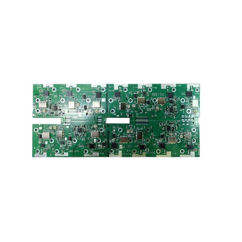
The industrial control board PCBA as the core component of industrial control, its characteristics i