Guangzhou Huachuang Precision Technology Co., Ltd. – Your Go-To Partner for High-Quality PCBA Solutions
Guangzhou Huachuang Precision Technology Co., Ltd. is a leading PCBA manufacturer offering high-qual
In modern PCBA (Printed Circuit Board Assembly), space efficiency, thermal management, and signal integrity are often top priorities. That’s where the QFN package with lid comes into play. QFN (Quad Flat No-Lead) packages are already renowned for their compact footprint and excellent thermal performance, but adding a lid — whether ceramic or plastic — unlocks even more capabilities for high-reliability and high-frequency applications.
For OEM engineers, procurement managers, and end-customers in Europe and North America, understanding exactly what a QFN package with lid offers (and what challenges it presents) is critical. Choosing an experienced PCBA supplier who knows how to handle such packages can dramatically reduce defect rates, improve thermal performance, and ensure regulatory compliance.
In this guide, HCJMPCBA covers everything you need to know: definition, construction, types, applications, challenges — and the six key criteria to evaluate PCBA suppliers when working with QFN-with-lid packages.
A QFN (Quad Flat No-Lead) package is an integrated circuit package characterized by a flat, lead-frame-based body without protruding leads, and it’s soldered directly to the PCB through pads under the package.
When the QFN comes with a lid, it typically means there is a cover (lid) — often ceramic or plastic — that encloses the die and internal components, forming either a sealed cavity or a more rugged package. This lid improves mechanical protection, hermeticity, and sometimes thermal stability.
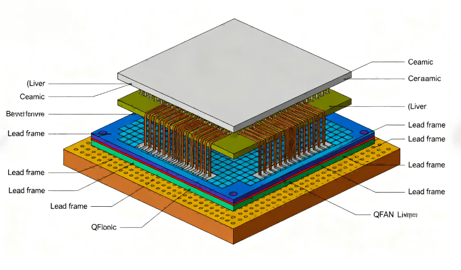
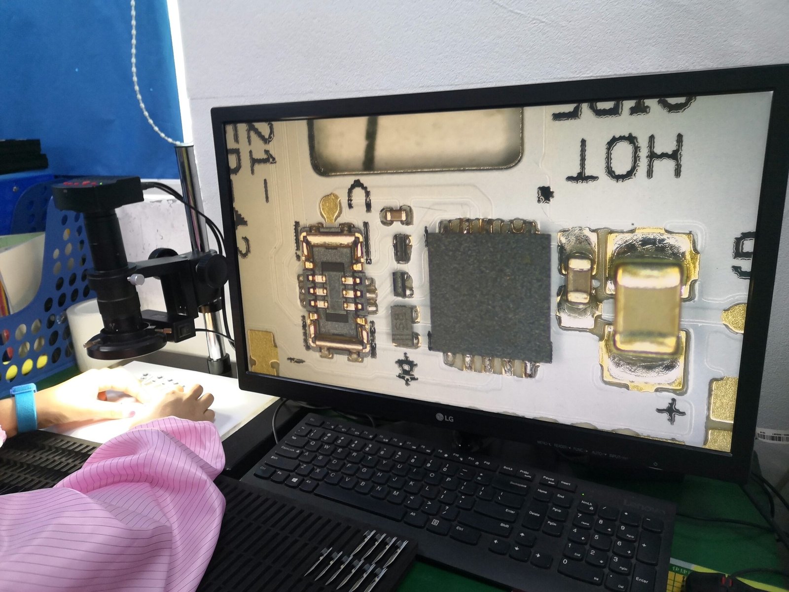
Hcjmpcba Cross Sectional View Of Qfn Structure
A typical QFN-with-lid package includes:
A copper leadframe (or lead-frame) that forms the internal electrical structure.
The die (IC chip), often attached to a central exposed pad (also called thermal pad).
Bond wires (e.g., gold or copper) connect the die to the leadframe.
Encapsulation material: for plastic QFNs, an epoxy or mold compound; for some with lid, the body may be plastic or even have an air cavity.
Lid: could be ceramic, plastic, or even metal; in air-cavity QFNs, the lid forms a cavity that helps in RF / microwave performance.
Exposed bottom pad: the package often has a large exposed pad on its underside, which is soldered to a PCB thermal landing to provide efficient heat dissipation.
Miniaturization and Compactness
QFN packages are very small and thin. According to Infineon, QFN uses significantly less PCB area compared to leaded packages like QFP.
Electrical Performance
The short bond wires and no external long leads result in low parasitic inductance and capacitance, making QFN very suitable for high-speed or high-frequency designs.
Thermal Performance
The exposed pad underneath the QFN provides a robust thermal path to the PCB.
When paired with a lid, especially ceramic ones, thermal stability and reliability can further improve, because the lid helps protect the die and maintain package integrity under thermal cycling.
Mechanical / Environmental Protection
A lid can provide mechanical protection and hermeticity (in ceramic-lid or air-cavity designs), making the package more robust in harsh environments.
Compliance
Many QFNs are RoHS-compliant (lead-free) and use modern lead-frame technologies.
Understanding the types of QFN-with-lid packages helps in selecting the right one for your application.
Plastic Molded QFN with Lid:
These are common, cost-effective. The body is molded in plastic, and a lid (plastic or sometimes ceramic) is used for mechanical protection.
Air-Cavity QFN (with Lid):
These packages have an internal cavity (air gap) and a lid (ceramic or plastic). This design is often used in RF / microwave applications because the cavity can improve high-frequency performance.
Ceramic QFN with Lid:
High-reliability applications often use ceramic lids. Such packages support robust thermal cycling, hermetic sealing, and long-term reliability.
Punch / Stamped QFN: Leadframe is punched for low-cost or low-volume production.
Saw-Singulated QFN: Leadframe is sawn; common for high-volume production.
Wettable Flank QFN: Sides (flanks) of the QFN are designed to be wettable during soldering, enabling better visual inspection of solder joints (especially useful in QA).
Flip-Chip QFN (fc-QFN): The die is flipped (face-down), typically bonding directly to the leadframe or substrate — very efficient for thermal and electrical performance.
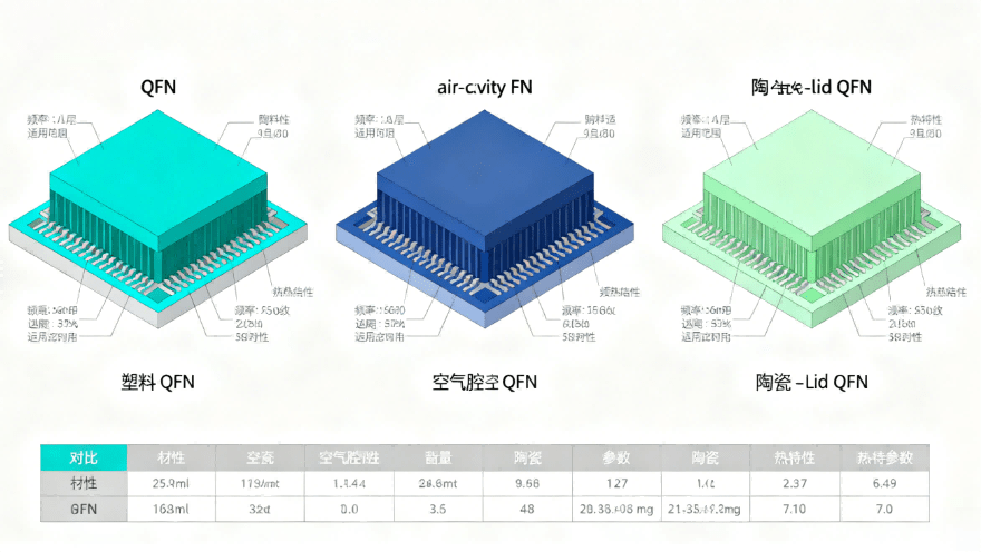
Hcjmpcba Comparison Chart Of Various Qfn Types
Where do QFN-with-lid packages shine in real-world PCBA?
High-frequency / RF Applications: Air-cavity QFNs with lids are excellent in microwave and RF modules, where signal integrity and low parasitics matter.
Automotive Electronics: Engine control units (ECUs), sensors, and modules benefit from the thermal stability and robustness of lid-equipped QFNs.
Industrial & IoT Devices: Compact, high-reliability PCBA boards in industrial settings often require rugged packaging.
Consumer Electronics: While cost-sensitive, premium or performance devices may choose QFN-with-lid to balance size and thermal performance.
Medical Devices: Hermetic ceramic-lid QFNs can be used in medical electronics where long-term reliability and environmental protection are required.
While QFN-with-lid packages offer many advantages, they also bring challenges in PCBA assembly. Understanding these is essential when choosing a supplier.
Assembly Precision
Because there are no side leads, accurate pick-and-place and stencil printing are critical. Misalignment or insufficient solder paste can lead to solder defects.
Inspection Difficulty
The solder joints (especially the bottom pad) cannot be visually inspected easily. Therefore, X-ray or specialized inspection is often needed.
Thermal Cycling Stress
Without flexible leads, QFN packages are more susceptible to fatigue under repeated temperature cycles.
The presence of a lid (especially rigid lids) requires careful thermal design, including via placement in the PCB to relieve stress.
Footprint Design
The PCB footprint must be carefully designed according to manufacturer recommendations (DFM). This includes thermal pad design, via array, solder mask, and paste windowing.
Cost Considerations
Lid-equipped QFNs (especially ceramic or air-cavity ones) are more expensive than standard plastic QFNs. Plus, inspection and process requirements add cost.
Hcjmpcba Cross Sectional View Of Qfn Structure
To ensure high-quality assembly of QFN packages with lids, here are six critical criteria to evaluate potential PCBA suppliers:
Technical Capability & Process Control
Does the supplier have high-precision placement machines capable of handling QFN bottom-pad packages?
Can they optimize reflow profiles for lids and thermal pads?
Do they support optimized stencil design for paste deposition under the thermal pad?
Inspection & Quality Assurance
Does the supplier use X-ray inspection or other non-visual methods to verify solder joints under the package?
Do they perform reliability testing (e.g., thermal cycling, solder joint shear) to validate lid integrity?
Design & DFM Support
Can the supplier provide DFM feedback for the PCB footprint, including thermal pad, via array, paste window, etc.?
Do they help optimize for the specific QFN variant (ceramic lid, air cavity, wet flanks)?
Regulatory & Material Compliance
Are the QFN parts and assembly process RoHS / REACH compliant?
Can the supplier source and verify quality of the QFN package with lid (e.g., certifying the lid material)?
Supply Chain & Capacity
Does the supplier have stable access to QFN-with-lid components?
Can they support low- to high-volume production?
Is lead time reasonable, and can they accommodate rush samples?
Technical Support & After-Sales Service
Do they offer support for process setup, troubleshooting, and assembly optimization?
In case of defects, do they have rework capabilities or experience dealing with lid packages?
Here are two practical tools you (or your procurement / engineering team) can use to evaluate potential PCBA suppliers:
Equipment: Placement machine precision, reflow oven zones, X-ray inspection.
Quality System: Certifications (ISO 9001, IPC), reliability testing protocols.
Engineering Support: DFM feedback, design review.
Service: Technical consulting, defect resolution, rework capabilities.
Solder Joint Reliability: Thermal cycling (e.g., –40 °C to +125 °C) to evaluate solder fatigue.
Mechanical Test: Shear or pull test on the QFN lid packages.
Functional & Signal Testing: Verify electrical function, especially for RF / high-speed QFNs.
Thermal Performance: Measure junction-to-board thermal resistance if applicable.
“All QFNs are the same” → False. QFNs with lids (especially ceramic or air-cavity) have very different behaviors from standard plastic QFNs in terms of thermal, mechanical, and RF performance.
“A lid-equipped QFN is just more expensive without benefit” → Not true. The lid can improve reliability, protect the die, and support high-frequency operation.
“Any PCBA house can handle QFN with lid easily” → No. Suppliers need specific capabilities (high-precision placement, X-ray, design feedback) to reliably assemble lid packages.
Q1: What’s the difference between a QFN with lid and without lid?
A: A lid (ceramic or plastic) provides mechanical protection, potential hermetic sealing, and sometimes enhanced thermal or RF performance, compared to lid-less QFNs.
Q2: Can QFN-with-lid packages be reworked?
A: Yes — but rework requires skill, proper thermal profiles, and may involve X-ray inspection. Not all PCBA manufacturers support lid rework.
Q3: Is a ceramic-lid QFN necessary for automotive / high-reliability use?
A: It depends. Ceramic lids offer better mechanical strength and hermeticity, which may benefit high-reliability or high-temperature environments. But a high-quality plastic-lid QFN could suffice for many designs.
Q4: How should I design my PCB footprint for a QFN with lid?
A: Follow the component manufacturer’s guidelines: include a thermal pad, use properly spaced vias under the pad, define the paste window carefully, and ensure solder mask clearance. Many PCBA suppliers can review your DFM.
A QFN package with lid offers a powerful combination of miniaturization, thermal efficiency, and reliability — especially for demanding applications like RF modules, automotive electronics, and industrial systems. But to fully realize its benefits, it’s essential to partner with a PCBA supplier that has deep experience and strong technical capabilities.
When evaluating suppliers, focus on the six key criteria: placement and process control, inspection, DFM support, regulatory compliance, supply stability, and engineering service. Use structured tools like audit checklists and sample testing to validate their competence.
By doing so, you can minimize risk, maximize yield, and ensure your product’s long-term performance.
Call to Action: To learn more about PCBA assembly of QFN packages with lid (including design support, reliability testing, and full assembly capabilities), please contact Guangzhou HCJM Precision Technology (HCJMPCBA).
Guangzhou Huachuang Precision Technology Co., Ltd. is a leading PCBA manufacturer offering high-qual
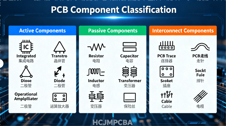
Introduction – Why Circuit Board Components Define PCB Performance & Supply Chain Value A bare
Guangzhou Huachuang Precision Technology Co., Ltd. (HCJMPCBA) is a leading ISO 13485-certified PCB


