Advanced Aluminum Substrate LED Light Boards & Electronics Manufacturing Solutions
Guangzhou Huachuang Precision Technology Co., Ltd. offers diverse electronics manufacturing solution
What Are Mouse Bites in PCB? A Step-by-Step Guide by HCJMPCBA
Table of Contents
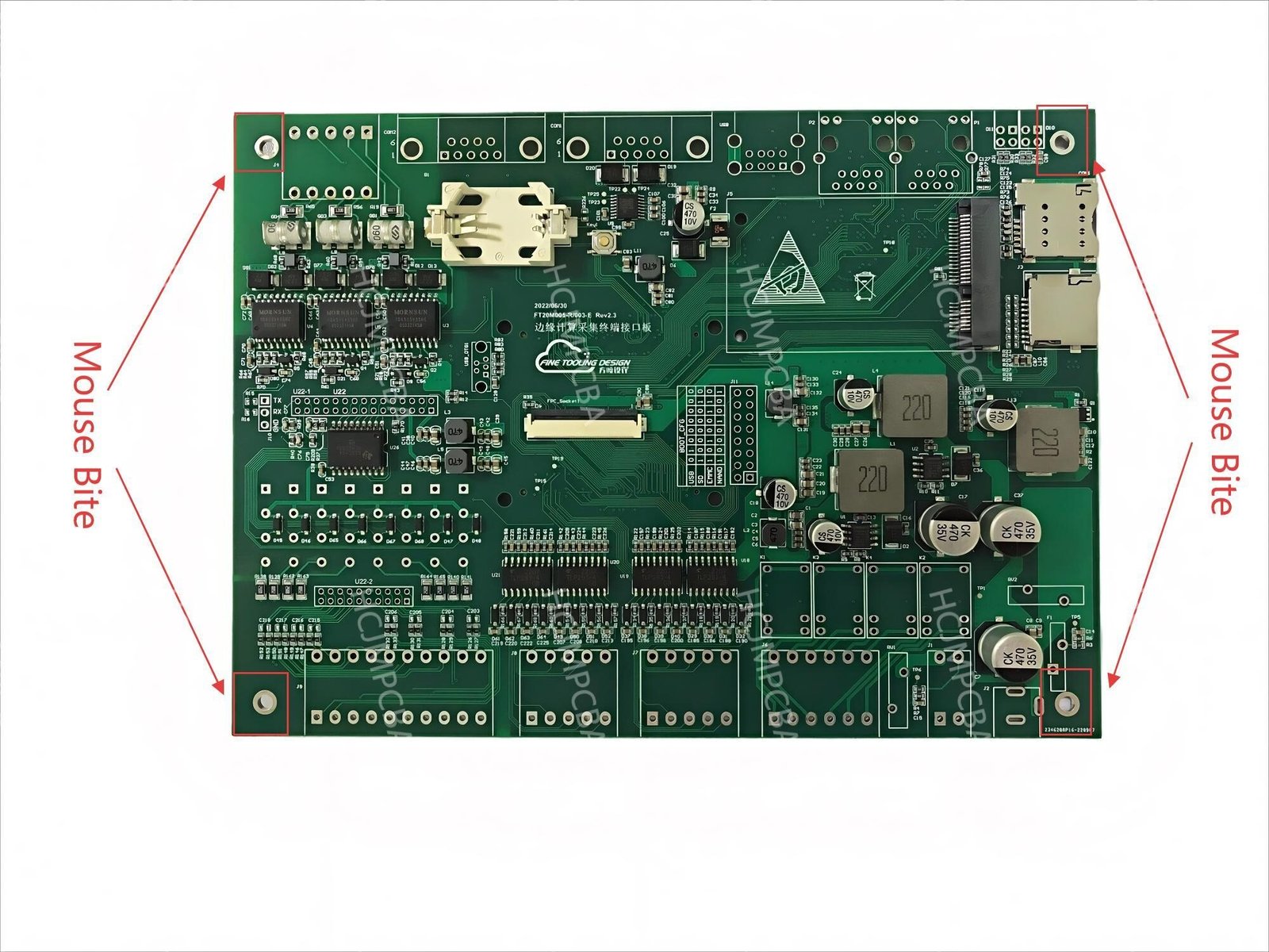
ToggleWhen panelizing printed circuit boards, you might come across perforated holes along the edge that look like tiny teeth—these are called mouse bites. Used widely in the electronics industry, mouse bites simplify board separation without complex tooling. In this post, HCJMPCBA breaks down everything you need to know about mouse bite panelization—from the what and why to design guidelines and supplier selection—so you can make informed decisions for PCBA fabrication.
A mouse bite is a series of small drill holes or perforations along the edge of a PCB panel, enabling easy separation of individual boards. Called mousebites, mouse bites PCB, or simply bite of mouse, this technique is also known as tab-routing depanelization.
Fabricators use mouse bites when dealing with irregular board shapes or special assembly requirements. They’re common when V-grooves can’t be used due to shape complexity or component placement constraints.

Mouse bites connect multiple PCBs within a panel using small tabs. Here’s how they function:
1.Hole Pattern – Typically 5 to 8 holes, ~0.5–0.6 mm in diameter, spaced ~0.35–0.4 mm edge-to-edge.
2.Placement Strategy – Place in panel blank areas, avoiding traces or components. At least two sets per panel side for stability. adding sets every 50–60 mm.
3.Panel Clearance – Maintain 1.2–2 mm spacing between boards; thinner panels need more margin to prevent breakage.
Design tools like Altium support mouse bite layout generation and embedded board array configuration.
Advantages:
1.Suitable for irregular shapes—unlike V-grooves, mouse bites work on complex outlines.
2.No extra tooling—drilling holes uses existing PCB processes.
3.Cost-effective for high-volume boards.
Drawbacks:
1.Separation may leave serrated edges requiring manual deburringjlcpcb.com.
2.Increased mechanical stress near edges—needs more careful design.
3.Not ideal for ultra-clean finishes or cosmetic-sensitive boards.
Here’s how mouse bites compare to other common methods:
| Method | Pros | Cons |
|---|---|---|
| Mouse Bites | Flexible for irregular shapes | Rough edge finish, needs post-processing |
| V-Scoring | Fast separation, clean edges | Only straight breaks, limited in shapes |
| Breakaway Tabs / Routing | Better edge quality, handles curves | More costly, requires CNC tools |
V-grooving works well for standard rectangular boards, while mouse bite panelization shines in custom and high-density applications.
Use these design tips to optimize mouse bite depanelization:
1.Maintain Clearance – Keep at least 1.5–2 mm from mouse bites to copper, components, or routing.
2.Hole and Spacing Specs – Follow 0.5–0.6 mm hole diameter, 0.35–0.4 mm spacing; limit to 5–8 holes per tab.
3.Symmetrical Placement – Balance panel strength by placing mouse bite sets opposite each other.
4.Tooling Marks & Fiducials – Use dedicated layers (e.g., in Altium) to define mouse bite and tooling positions for manufacturability.
5.Smooth Separation – Plan for edge cleanup steps post-depanelization, such as light filing or polishing.
To select top-tier suppliers for mouse bite implementation, evaluate these criteria:
1.Panelization Capabilities – Ability to produce mouse bite panels for irregular shapes seamlessly.
2.Precision Drilling – High-accuracy CNC or laser systems to maintain tight hole specs.
3.Process Consistency – Ensure consistent hole patterns across production batches.
4.Experience with Edge Finishing – Ability to offer post-depanel edge cleanup or smoothening.
5.Full Turnkey Services – From design-for-manufacturing (DFM) to assembly and testing—this ensures your mouse bite PCBs maintain structural integrity and functionality.
1.Mouse bite refers to small perforations used in PCB panelization, enabling easy breakup of multiple boards without complex tools.
2.It’s ideal for irregular shapes, high-volume builds, or thin boards.
3.Design for proper hole sizing, spacing, and component clearance to avoid mechanical failures.
4.Evaluate suppliers on both design capabilities and panel handling expertise.
5.By mastering the details of mouse bite depanelization, engineering teams and procurement stakeholders can ensure both performance and manufacturability in their electronics products.
Learn more about PCBA services, contact Guangzhou Huachuang Precision Technology.
Guangzhou Huachuang Precision Technology Co., Ltd. offers diverse electronics manufacturing solution
Discover what does PCB stand for in this comprehensive guide by HCJMPCBA. Learn about ict tester rol
The electronics manufacturing industry is undergoing significant changes driven by technological adv