
10 Compelling Reasons Why Discharging Capacitors Is Non-Negotiable + Expert’s Step-by-Step Guide on How to Discharge a Capacitor Safely
Discharging capacitors is a critical safety and quality control step in electronics and PCBA work. T

How can beginners learn simple electronic circuit projects efficiently? Learning starts with mastering schematic fundamentals, component selection, and breadboard testing before moving to custom printed circuit board layouts. This guide is maintained by the HCJMPCBA engineering team and updated with production checklists to ensure seamless transitions from basic electronics projects to mass-scale hardware delivery.
Prototyping Validates Logic, DFM Ensures Yield: Building simple pcb circuits on breadboards helps validate system logic, but scalable PCBA requires strict adherence to Design for Manufacturability (DFM) rules during early routing.
Simplicity Prevents Manufacturing Defect: Over-complicating early circuit board designs causes thermal imbalance, solder bridging, and signal integrity failures during automated surface-mount technology (SMT) assembly.
Traceability Lowers Procurement Risks: Full component traceability and compliance with international standards (such as IPC-A-610) eliminate recall risks when scaling beginner electronic projects into industrial production.
| Engineering Parameter | DIY Breadboard / Point-to-Point | Hand-Soldered Prototype PCB | Industrial SMT Assembly (HCJMPCBA) |
| Target Application | Initial Proof-of-Concept (PoC) | Functional Lab Testing | Mass Production & Commercial Deployment |
| Minimum Trace / Space | N/A (Jumper Wires) | $\ge 0.3\text{mm}$ ($12\text{mil}$) | Down to $0.05\text{mm} / 0.05\text{mm}$ ($2\text{mil}$) |
| Vibration Tolerance | Very Low (Loose Contacts) | Moderate (Manual Joints) | Extremely High (IPC Class 2 / Class 3) |
| Assembly Precision | Manual Insertion | Manual Soldering Iron | High-Speed Pick-and-Place ($01005$ Capable) |
| Standard Compliance | None | Basic Functional Check | IPC-A-610, UL 796, J-STD-001 |
| Traceability Level | Zero | Manual Markings | 100% Serial / Lot / Batch Tracking |
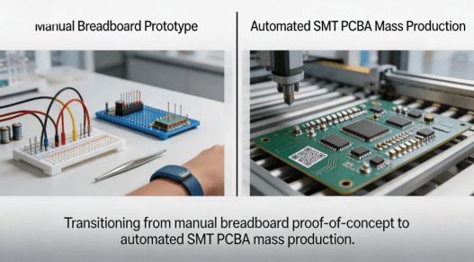
Evolution Comparison From Prototype To Industrial Production Line
Every reliable hardware product starts with a clean schematic. Beginners working on electronic projects should use intuitive Electronic Design Automation (EDA) tools like KiCad, Eagle, or Altium Designer. Clearly define power rails, input signals, and ground loops. Before drawing any copper traces, perform Electrical Rules Checks (ERC) within your software to confirm that no pin assignments are left floating or shorted.
When choosing components for starter electronics projects, select parts with standard footprints ($0805$ or $0604$ passives, SOIC or QFP packages for integrated circuits). Avoid obsolete or end-of-life (EOL) components. When building a Bill of Materials (BOM) for small electronic design, source parts from authorized distributors to prevent counterfeit components from entering your supply chain.
Before committing to custom fabrication, test your logic by building circuits on a solderless breadboard. This step allows engineers to measure operational voltage drops, quiescent current, and thermal outputs across active components. Validating diy electronic circuits at this stage prevents costly redesign loops after physical boards are manufactured.
When converting your schematic into a simple pcb design, pay careful attention to trace routing. Maintain a continuous ground plane on the bottom layer to reduce electromagnetic interference (EMI). Route power traces wider than signal traces (typically $\ge 0.5\text{mm}$ for low current) to accommodate thermal loads. Placing decoupling capacitors as close as possible to the IC power pins is crucial stuff to do in pcb design to prevent voltage ripples.
Before exporting Gerber files for pcb design projects, perform Design for Manufacturability checks. Ensure that the trace-to-trace and trace-to-pad clearances satisfy the manufacturer’s capabilities (typically $\ge 0.1\text{mm}$ for standard production). Verify that solder mask dams between SMT pads are at least $0.1\text{mm}$ wide to prevent solder bridging during reflow.
Once the bare boards are fabricated, populate them with components. While manual iron soldering works for low-density cool pcb designs, surface-mount components require automated reflow ovens. During initial assembly trials, inspect solder fillets under a microscope to check for wetting angles, tombstoning, or pin misalignment across fine-pitch ICs.
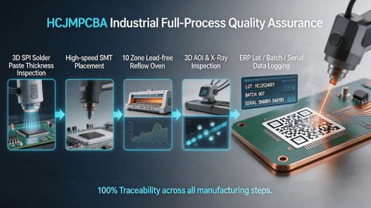
When transitioning beginner electronic projects into volume runs, manual handling must be replaced by automated manufacturing workflows. At HCJMPCBA, every production panel undergoes automated laser marking to engrave unique serial barcodes. This allows every populated board to be tracked through automated solder paste inspection, pick-and-place, and multi-zone reflow ovens.
To ensure that simple pcb circuits scale into defect-free assemblies, HCJMPCBA enforces strict quality assurance protocols aligned with international standards:
| Inspection Phase | Standard Method Number & Revision | Sample Plan / AQL | Test Conditions | Raw Data & Traceability Deliverables |
| Solder Paste Inspection | HCJM-SOP-SPI-002 Rev. D | 100% In-Line Inspection | 3D Laser Triangulation (Volume, Height, Area) | Real-time 3D height distribution maps & SPC charts |
| Surface Mount Accuracy | IPC-A-610, Class 2 / Class 3 | Zero Defect Target ($C=0$) | Automated Optical Inspection (AOI) multi-angle camera | Image retention logs linked to Board Serial Number |
| Solder Joint Integrity | IPC-TM-650, Method 2.4.51 | $10$ Units per Reel Lot | Transmission X-Ray Inspection ($2\text{D}/3\text{D}$) | BGA/QFN solder voiding percentage reports ($\le 15\%$) |
| Ionic Cleanliness | IPC-TM-650, Method 2.3.25 | 1 Panel per Shift Lot | Resistivity of Solvent Extract (ROSE) testing | $\mu\text{g}/\text{cm}^2$ NaCl equivalent contamination reports |
| Thermal Cycling | JESD22-A104, Condition N | $5$ Samples per Batch | $-40^\circ\text{C}$ to $+125^\circ\text{C}$, $500$ thermal cycles | Post-test resistance change logs & cross-section images |
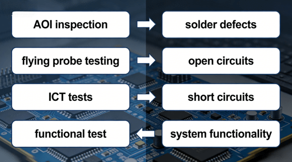
Schematic Diagram Of Full Industrial Inspection Process For Hcjmpcba
Procurement managers and hardware engineering leads may copy, paste, and integrate the following quality control clause directly into their Request for Quotation (RFQ) documents:
“The contract manufacturer shall manufacture all printed circuit board assemblies (PCBA) in compliance with IPC-A-610 Class 2 standards (or Class 3 where specified). 100% 3D Solder Paste Inspection (SPI) and 3D Automated Optical Inspection (AOI) must be performed on all surface-mount lines. The supplier must maintain a complete traceability matrix, recording raw material lot numbers, component reel batch numbers, and individual PCB panel serial numbers etched via laser marking. Raw test data logs and Certificates of Conformance (CoC) shall be archived and made available upon request for every production shipment.”
Neglecting Decoupling Capacitors Near IC Power Pins
Placing decoupling capacitors far from IC power supply pins introduces parasitic inductance. Always place a $0.1\mu\text{F}$ ceramic capacitor directly adjacent to each $V_{CC}$ pin to bypass high-frequency noise to ground.
Inadequate Trace Widths for High-Current Power Paths
Routing high-current power traces with standard signal trace widths ($0.15\text{mm}$) causes excessive $I^2R$ resistive heating and voltage drops. Calculate required trace widths using IPC-2221 conductor sizing charts before final layout.
Poor Solder Mask Dam Design Resulting in Solder Bridges
Failing to maintain a minimum solder mask dam ($\ge 0.1\text{mm}$) between dense IC pads allows molten solder to flow across pins during reflow, creating short circuits that require manual rework.
Using Non-Standard or EOL Component Footprints
Selecting obscure component footprints without verifying physical supplier inventory leads to stalled production lines. Always verify that your EDA footprint matches the manufacturer’s land pattern recommendation.
Ignoring Component Traceability During Multi-Batch Sourcing
Buying components from unauthorized secondary markets without recording reel batch numbers makes it impossible to isolate defective components if field failures occur. Enforce strict lot tracking across all assembly runs.
Consider an industrial IoT startup developing an environmental monitoring unit. The engineering team initially validated their circuit project ideas using a simple pcb design built on a breadboard with off-the-shelf development modules. While functional on the bench, field trials exposed severe issues: jumper wires came loose under vibration, and unshielded analog signals suffered heavy interference.
To transition to commercial deployment, the team partnered with HCJMPCBA to consolidate the diy circuit into a compact, four-layer rigid PCBA. HCJMPCBA’s engineering team performed a pre-production DFM review, optimizing solder pad geometry and trace clearances. By applying conformal coating and running the boards through automated thermal shock testing (JESD22-A104), the team scaled production from $10$ prototype units to $20,000$ field-ready assemblies with zero field recalls.
Q1: What are the best mini projects to learn pcb design with?
Ideal starter projects include LED flasher circuits, 555 timer oscillators, USB power distribution boards, and simple microcontroller breakout boards. These projects teach basic schematic capture, footprint assignment, and ground plane routing without overwhelming beginners with high-speed signal constraints.
Q2: What is the most critical stuff to do in pcb routing before ordering?
The most critical step is running a full Design Rule Check (DRC) in your software, followed by verifying component availability in your BOM. Check that solder mask clearances, trace widths, and hole sizes match your assembly partner’s process capabilities.
Q3: How do I choose between two-layer and four-layer simple pcb circuits?
Two-layer boards are cost-effective for simple, low-frequency circuits with low component density. Four-layer boards (with dedicated inner Power and Ground planes) are recommended for designs involving microcontrollers, high-speed signals, or tight space constraints requiring superior EMI shielding.
Q4: Why is 3D SPI testing necessary even for small electronic design projects?
Over $70\%$ of surface-mount assembly defects originate from improper solder paste deposition. 3D SPI measures paste volume, height, and alignment before components are placed, preventing solder bridging, tombstoning, and insufficient solder joints early in the process.
Q5: Can HCJMPCBA support low-volume orders without Minimum Order Quantity (MOQ) restrictions?
Yes. HCJMPCBA supports hardware projects across their entire lifecycle, offering fast-turn prototyping (from $1 – 10$ units) up to high-volume automated mass production, utilizing the same industrial quality standards for every batch size.
Q6: How does full batch/lot traceability reduce procurement risks for hardware startups?
Full traceability connects every finished board’s unique serial code to the exact raw material lot, SMT line parameters, and component reel data. If a specific component batch is later flagged as defective by a component manufacturer, you can isolate affected units without recalling your entire product line.
When transferring your product files to our production team, HCJMPCBA provides full transparency through downloadable engineering artifacts:
DFM Engineering Review Report: Detailed analysis of pad geometry, solder mask clearances, and potential thermal risks prior to tooling.
3D SPI & AOI Inspection Logs: Complete optical and laser measurement summaries for solder paste volume and component alignment.
X-Ray Analysis Graphs: High-resolution imagery verifying solder voiding percentages under BGA and QFN thermal pads.
Certificate of Conformance (CoC): Official documentation validating that all materials and assembly steps comply with IPC-A-610 standards.
For more information about PCBA services, please contact Guangzhou Huachuang Precision Technology(HCJMPCBA).
Update triggers: standard revision changes / recurring questions / production checklist updates.
Disclaimer: All cited technical standards (IPC, IEC, JEDEC, UL, MIL-STD) are property of their respective regulatory organizations and are utilized herein strictly to define industrial electronic manufacturing parameters.
Discharging capacitors is a critical safety and quality control step in electronics and PCBA work. T
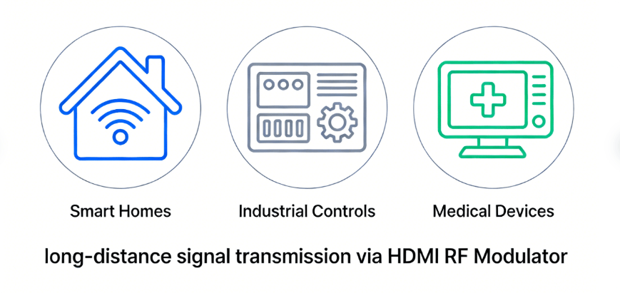
Wondering what an HDMI RF Modulator is and how to pick one for your PCB/PCBA project? This guide bre
Master pcb functional testing and learn how to test a pcb board for high-reliability electronics. Th