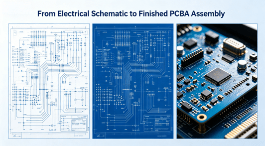
What Is an Electrical Schematic? 9 Practical Steps to Read a Circuit Diagram and Understand How PCBs Are Manufactured
Learn what an electrical schematic is, how to read a circuit diagram, and how PCB/PCBA manufacturing
Zero-Defect Stencil Printing: A Comprehensive Guide to PCBA Solder Paste Precision (2026 Updated)
Table of Contents
ToggleStencil printing is one of the most critical steps in SMT assembly because every downstream solder joint depends on the accuracy of the solder paste deposit. If paste volume, height, shape, or position is unstable, even the best placement machine and reflow oven cannot fully recover the process. At HCJMPCBA, we use 100% 3D SPI closed-loop control, precision stencil engineering, and production data feedback systems to keep printing defect rates below world-class targets in demanding builds such as Robotics PCBA, industrial controls, and high-density electronics.
This guide is maintained by the HCJMPCBA SMT engineering department, integrating 20+ years of production raw data and IPC-7527 standards.
Many buyers compare factories by unit price, lead time, or machine brand. However, experienced engineers know the real yield battle often starts before component placement.
A poor solder paste print can create:
In practical manufacturing terms, stencil printing often determines whether the assembly line runs smoothly or spends hours in rework.
For robotics electronics, the consequences are even greater. A weak solder joint on a sensor interface or motor driver board may not fail immediately—but it can fail after vibration, thermal cycling, or repeated duty in the field.
High-Precision Solder Paste Inspection (3D SPI) At HCJM, we don’t just print; we measure. Our 3D SPI systems provide full-volume analysis of every solder deposit, ensuring precision for ultra-fine pitch components like BGA, QFN, and 01005.
Why It Matters for Your Project:
Closed-Loop Integration: Our SPI communicates in real-time with screen printers to automatically adjust offsets, minimizing human error.
SPC Real-Time Monitoring: We utilize Statistical Process Control (SPC) to track height and volume trends, predicting potential defects before they occur.
Mass Production Consistency: By catching 70% of potential soldering issues at the first stage, we achieve higher first-pass yield (FPY) and faster turnaround for high-volume orders.
A large share of soldering defects originate upstream from unstable paste deposits rather than from the reflow oven itself. Control the print, and downstream yield improves dramatically.
3D solder paste inspection catches defects before components are mounted. That means defects are corrected at the lowest-cost stage.
Nano-coated apertures, laser-cut geometry, and controlled release behavior significantly improve automated PCB assembly consistency, especially for fine-pitch and miniaturized products.
Good stencil printing is not just “paste on pad.” It means the deposit is controlled across multiple dimensions:
IPC-7527 provides industry guidance for evaluating solder paste printing quality and visual acceptability.
That matters because two factories may both claim “IPC quality,” yet one operates with tight statistical control while another reacts only after defects appear.
Bridging happens when adjacent deposits connect or spread excessively before reflow. This is common on fine-pitch ICs, QFPs, and dense connector pins.
For dense Robotics PCBA designs, bridging prevention is critical because one shorted signal pin can disable the entire control system.
Insufficient paste volume may create opens, weak joints, intermittent failures, or low mechanical strength.
Aperture release depends heavily on geometry and wall condition. If paste does not release consistently, the same board can show random variation pad to pad.
Solder balls may indicate contamination, excessive flux disturbance, moisture issues, or unstable thermal behavior.
Even when cosmetic, solder balls can indicate process instability. In sensitive products, loose particles may become a reliability risk.
Paste printed off-center can reduce wetting margins or create bridges.
Two deposits may look similar from above but differ significantly in height and volume.
This is why 2D inspection alone is often insufficient for advanced builds.
| Parameter | Standard Printing | HCJMPCBA Precision Printing |
|---|---|---|
| Pressure Setup | Operator experience | Window-controlled recipe |
| Print Speed | Generic setting | Product-specific optimization |
| Separation | Fixed | Tuned by board & aperture behavior |
| Inspection | Sampling / visual | 100% 3D SPI |
| Correction | Manual after defects | Closed-loop feedback |
| Stencil Type | Standard laser cut | Nano-coated / FG steel options |
| Data Output | Basic pass/fail | Volume / Height / Trend raw data |
| Metric | Industry Standard | HCJMPCBA Benchmark | Evidence for Client |
|---|---|---|---|
| Inspection Coverage | Manual / Sampling | 100% 3D SPI | Exportable raw data |
| Stencil Quality | Standard | Nano-coated options | Method number + revision |
| Traceability | Batch level | Serial / Unit capable | Lot/Batch/Serial records |
| Parameter Control | Setup only | Controlled recipes | Process logs |
| Trend Management | Reactive | SPC / alarms | Yield reports |
Before production begins, our engineers review:
The goal is to prevent defects before steel is cut.
Paste performance changes with storage abuse.
Our controls may include:
Before release:
After print, the board enters 3D SPI.
Measured values include:
If drift is detected, the system can trigger cleaning, offset correction, or engineer review before defects multiply.
This is one of the most effective ways to protect automated circuit board assembly yield.
These mistakes may not appear in prototypes but become expensive during mass production.
Many modern OEM programs require frequent changeovers:
In this environment, process discipline matters more than machine speed.
HCJMPCBA supports controlled changeover through:
Result: faster transitions without sacrificing print consistency.
Q1: How does humidity affect soldering robot performance?
Humidity can change paste behavior, increase slump risk, affect tackiness, and contribute to process instability. It also impacts stored materials if unmanaged.
Q2: Why insist on raw data for every SPI scan?
Because pass/fail hides trends. Raw data reveals drift before defects exceed limits.
Q3: What is the impact of stencil cleaning frequency?
Too little cleaning increases blockage and smear risk. Too much cleaning may reduce throughput unnecessarily. The right interval is product-dependent.
Q4: Is nano-coating worth the extra cost?
Often yes for fine-pitch, micro-aperture, and repeatability-critical builds where release performance matters.
Q5: Can a good reflow profile fix poor printing?
Only partially. Reflow cannot reliably compensate for missing, bridged, or badly placed deposits.
Q6: Why do prototype boards sometimes pass but production fails?
Small sample sizes may hide variation. Mass production exposes weak process windows.
Buyers evaluating suppliers can request:
Factories confident in their systems usually welcome evidence-based audits.
Price pressure is real. But the cheapest quote becomes expensive when it creates:
Stencil printing discipline is invisible on a quotation sheet—but visible in long-term total cost.
Reliable PCBA does not begin in the oven. It begins at the stencil.
When solder paste printing is engineered, measured, and continuously corrected, the rest of the SMT process becomes more stable, scalable, and predictable. That is especially important for robotics, industrial controls, medical electronics, and other products where failure is not acceptable.
Update triggers: standard revision changes / recurring questions / production checklist updates.
Learn what an electrical schematic is, how to read a circuit diagram, and how PCB/PCBA manufacturing

Medical PCB assembly is essential for creating reliable, high-precision electronic medical component
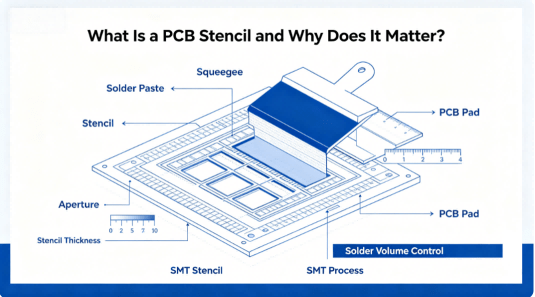
A PCB stencil controls solder paste deposition and directly affects SMT yield. Learn how solder past