Low MOQ, High Mix: Making HMLV PCBA Work Without the Volume Penalty
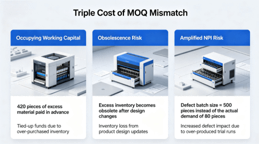
HMLV programs — 50 to 300 units per build — get squeezed by MOQ minimums that assume high-volume
Side plating (also known as PCB edge plating or edge metallization) is a PCB manufacturing process that deposits conductive copper and surface finish material along one or more board edges. It is commonly used to improve EMI shielding, grounding continuity, edge conductivity, and mechanical durability in advanced PCB and PCBA applications.
This guide is maintained by the HCJMPCBA engineering team and updated with production checklists.
In standard PCB manufacturing, conductive copper exists on surface layers, internal layers, plated through-holes, and vias. However, some applications require electrical continuity along the actual edge of the board.
Side plating is the process of extending conductive metal onto the routed edge of a PCB, creating a plated sidewall that becomes electrically connected to selected copper features.
The plated edge may connect directly to:
This technique is widely used in communication equipment, industrial control systems, RF modules, automotive electronics, and products that must meet strict EMC requirements.
| Feature | Standard PCB Copper | Side Plating |
|---|---|---|
| Location | Surface and internal layers | Board edge |
| Grounding Capability | Standard | Enhanced |
| EMI Shielding | Limited | Improved |
| Mechanical Reinforcement | Standard | Enhanced |
| Edge Conductivity | No | Yes |
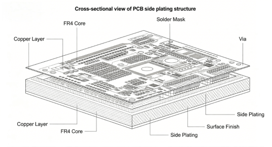
Cross Sectional View Of Pcb Side Plating Structure Hcjmpcba
One of the primary reasons engineers specify side plating is to improve electromagnetic compatibility.
High-speed digital circuits, RF devices, and communication equipment often generate unwanted electromagnetic emissions. A plated PCB edge can create a more continuous grounding structure around the perimeter of the board.
When combined with ground stitching vias, side plating helps reduce:
This can simplify EMC compliance testing and improve overall system robustness.
Ground continuity is critical in many industrial and communication products.
Side plating can help:
For products operating in electrically noisy environments, improved grounding often translates directly into better signal integrity.
PCB edges frequently experience mechanical stress during:
Side plating can provide additional reinforcement to board edges, especially when combined with robust PCB stack-up design.
As operating frequencies increase, electrical current tends to travel along conductor surfaces due to skin effect.
Because side plating creates additional conductive surfaces, it may contribute to improved RF grounding performance in certain applications.
Typical applications include:
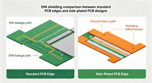
Emi Shielding Comparison Between Standard Pcb Edges And Side Plated Pcb Designs Hcjmpcba
Engineers sometimes confuse side plating with castellated holes. Although both involve conductive structures near the PCB edge, their purposes differ significantly.
| Feature | Side Plating | Castellated Holes |
|---|---|---|
| Edge Conductivity | Excellent | Partial |
| EMI Shielding | Excellent | Limited |
| Board-to-Board Connection | Limited | Excellent |
| Mechanical Reinforcement | Strong | Moderate |
| RF Grounding | Excellent | Moderate |
Castellated holes are typically used for module attachment, while side plating is primarily intended for grounding, shielding, and structural enhancement.
Rule 1 – Define Side Plating During PCB Layout
Side plating should be included during the initial PCB design stage. Late-stage requests often create manufacturing complications and redesign costs.
Rule 2 – Maintain Adequate Copper-to-Edge Clearance
Copper features must be positioned correctly relative to the routed edge to ensure plating continuity while preventing manufacturing defects.
Rule 3 – Provide Continuous Ground Connections
Ground copper should connect to the plated edge wherever shielding or EMC improvement is desired.
Rule 4 – Use Ground Stitching Vias
Closely spaced ground vias improve electrical continuity between internal layers and plated edges.
Rule 5 – Consider Panelization Requirements
Side plating often affects panelization methods and breakout strategies.
Designers should confirm manufacturing capability before finalizing board dimensions.
Rule 6 – Evaluate Surface Finish Compatibility
ENIG, immersion tin, immersion silver, and other finishes may influence final plating appearance and performance.
Rule 7 – Verify Mechanical Tolerances
Board-edge tolerances become increasingly important when side plating interfaces with metal enclosures or connectors.
Rule 8 – Avoid Isolated Copper Islands
Disconnected copper sections can create inconsistent plating quality and potential reliability concerns.
Rule 9 – Review Current-Carrying Requirements
If plated edges are expected to conduct significant current, additional analysis may be necessary.
Rule 10 – Define Inspection Criteria
Acceptance criteria should be documented before production begins.
Rule 11 – Control Manufacturing Revisions
Design updates affecting plated edges should be managed through revision-controlled documentation.
At HCJMPCBA, engineering reviews may include DFM verification, manufacturing feasibility analysis, and revision-controlled release procedures before production approval.
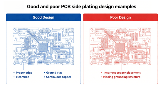
Good And Poor Pcb Side Plating Design Examples Hcjmpcba
Determine whether side plating is required for:
Not every board edge requires plating.
Engineers should define exactly which edges require conductive sidewalls.
Create intentional connections between the plated edge and the grounding network.
Manufacturing capabilities vary among PCB suppliers.
Confirm:
Routing and breakout methods must support reliable edge plating.
Specify:
For production builds, documentation should include:
| Application | Recommended | Primary Benefit |
|---|---|---|
| RF Module | Yes | EMI Control |
| Industrial Control | Often | Grounding |
| Automotive Electronics | Yes | Reliability |
| Communication Equipment | Yes | Shielding |
| Consumer Electronics | Depends | Cost vs Benefit |
| Medical Electronics | Often | EMC Compliance |
Side plating provides valuable benefits, but it also introduces manufacturing complexity.
Common challenges include:
The board edge must remain accessible during plating operations.
Poor copper balancing can affect plating consistency.
Edge quality directly influences final plating quality.
Some finishes require additional process control.
Side plating generally increases fabrication complexity compared with standard PCB construction.
Therefore, engineers should confirm that the performance benefits justify the additional manufacturing
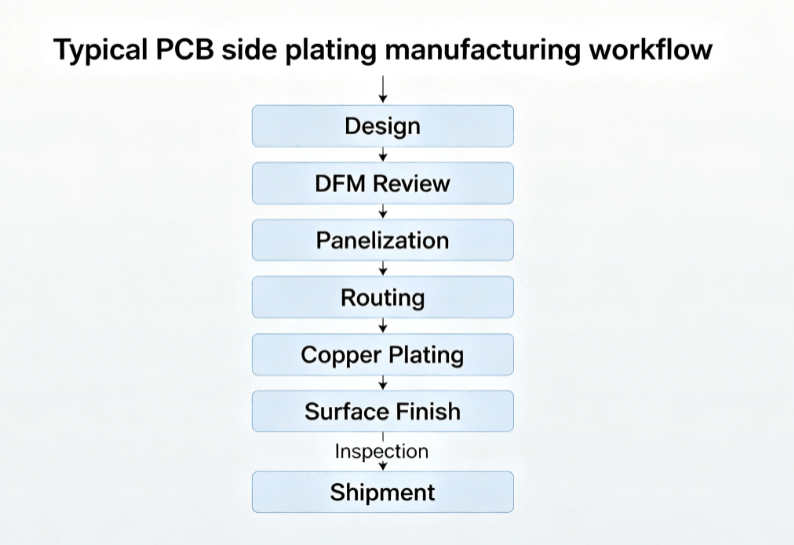
Typical Pcb Side Plating Manufacturing Workflow Hcjmpcba
| Verification Item | Evidence | Purpose |
|---|---|---|
| Plating Thickness | Cross-section Report | Reliability |
| Copper Continuity | Electrical Testing | Conductivity |
| Surface Finish | Inspection Report | Corrosion Resistance |
| Revision Control | Method Number + Revision | Change Control |
| Sample Plan | Inspection Records | Consistency |
| Test Conditions | Validation Records | Repeatability |
| Traceability | Lot/Batch/Serial Records | Root Cause Analysis |
| Raw Data | Measurement Records | Audit Support |
For controlled PCB and PCBA projects, HCJMPCBA can maintain manufacturing documentation linked to revision histories, inspection records, lot tracking, and production traceability requirements when specified by customer agreements.
Mistake 1 – Requesting Side Plating After Layout Completion
Late changes frequently require design modifications and manufacturing reevaluation.
Mistake 2 – Ignoring Ground Via Placement
Without proper grounding structures, side plating may deliver limited EMC benefit.
Mistake 3 – Insufficient Copper Clearance
Improper clearances can create fabrication risks.
Mistake 4 – Undefined Surface Finish Requirements
Different finishes may affect appearance and long-term performance.
Mistake 5 – Missing Verification Requirements
Without documented inspection criteria, acceptance standards become unclear.
An industrial communication device experienced excessive emissions during EMC testing.
Initial investigation revealed that grounding continuity around the board perimeter was insufficient.
The engineering team redesigned the PCB to include:
After verification and retesting, the revised design demonstrated improved shielding effectiveness and achieved compliance targets.
Although side plating was not the only design change, it contributed to a more continuous grounding structure and improved EMC performance.
Before approving production, OEM buyers may request:
These records provide objective evidence that manufacturing processes remain controlled and repeatable.
PCB supplier shall provide verification records demonstrating side plating continuity, plating thickness compliance, revision-controlled manufacturing documentation, and traceability records for applicable production lots. Inspection evidence shall be retained according to agreed project requirements.
HMLV programs — 50 to 300 units per build — get squeezed by MOQ minimums that assume high-volume

Learn how to read the resistor color code with our step-by-step guide. Decode 4-band and 5-band resi
PLC and industrial control boards are high-complexity, low-volume builds — 200+ part numbers, lots